-
What does Haibo do?
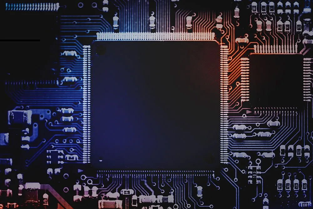
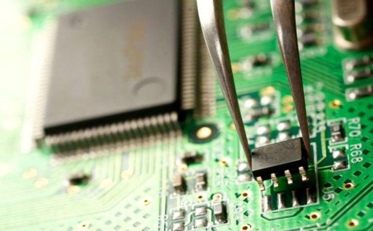
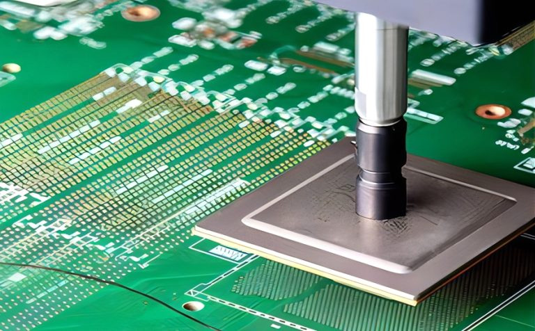
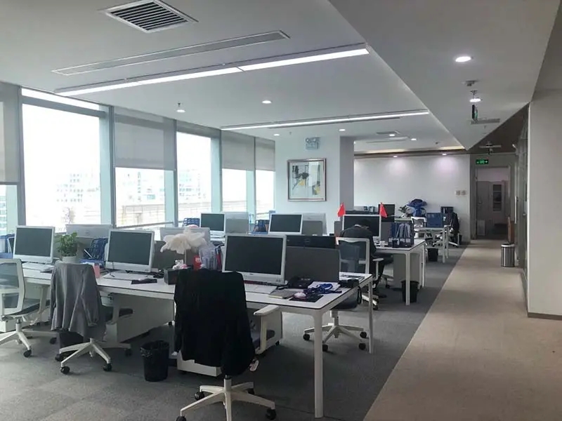
Haibo is a PCB board manufacturer that provides small and medium batch PCB circuit board, PCB assembly, and electronic manufacturing services, including electronic design, PCB layout, SMT and through-hole assembly, material procurement, final packaging, and project management. Finally, provide high-quality products and services.
-
What are the benefits of outsourcing my product to Haibo?
Since 2017, we have been a PCB supplier in China, and we have many customers who have been cooperating with us for more than 10 years! We demand that they provide the benefits of being a partner, which is simple: we are trustworthy! During the RFQ process, our CAM engineers will carefully examine all details and raise questions to avoid errors in the future. When customers order PCBs or PCB assemblies from us, we are always able to deliver high-quality products on time.
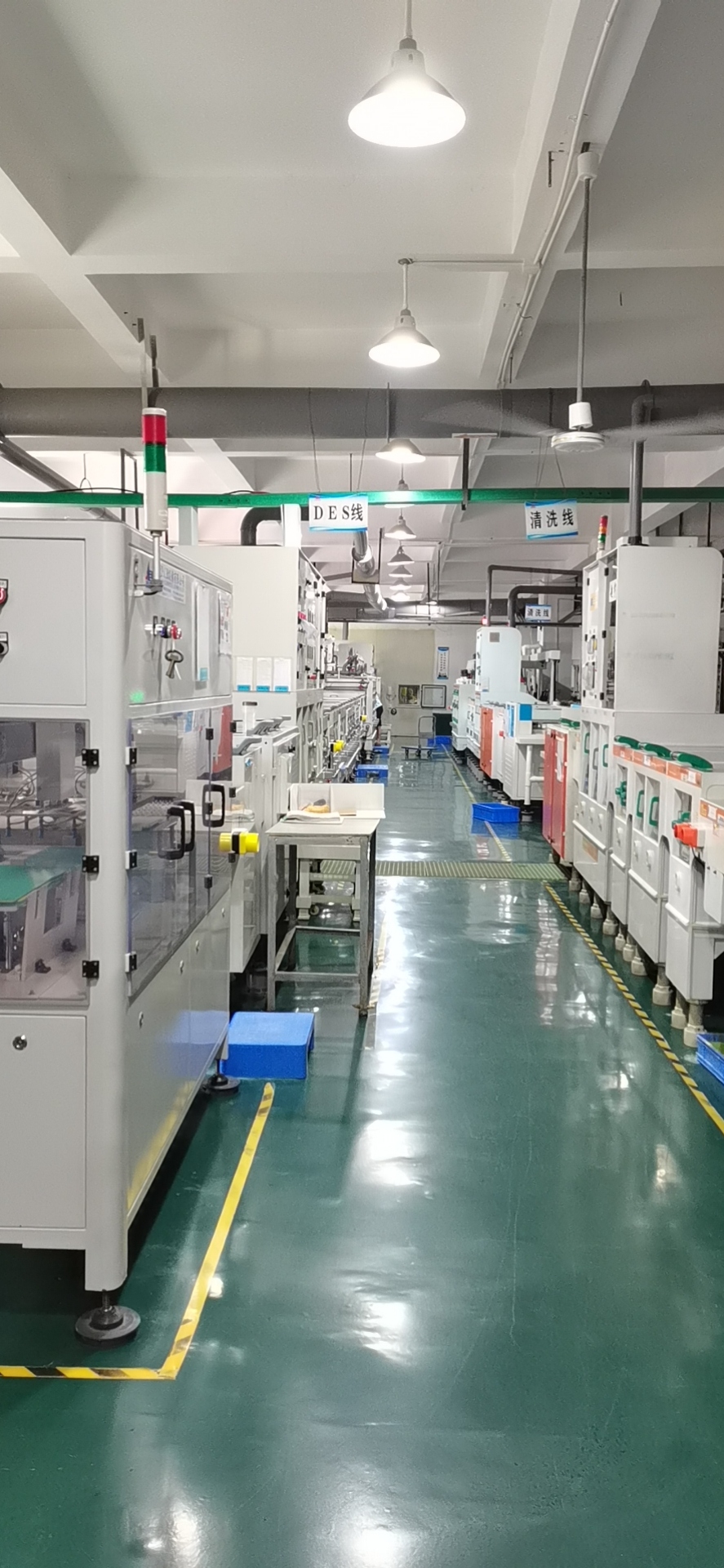
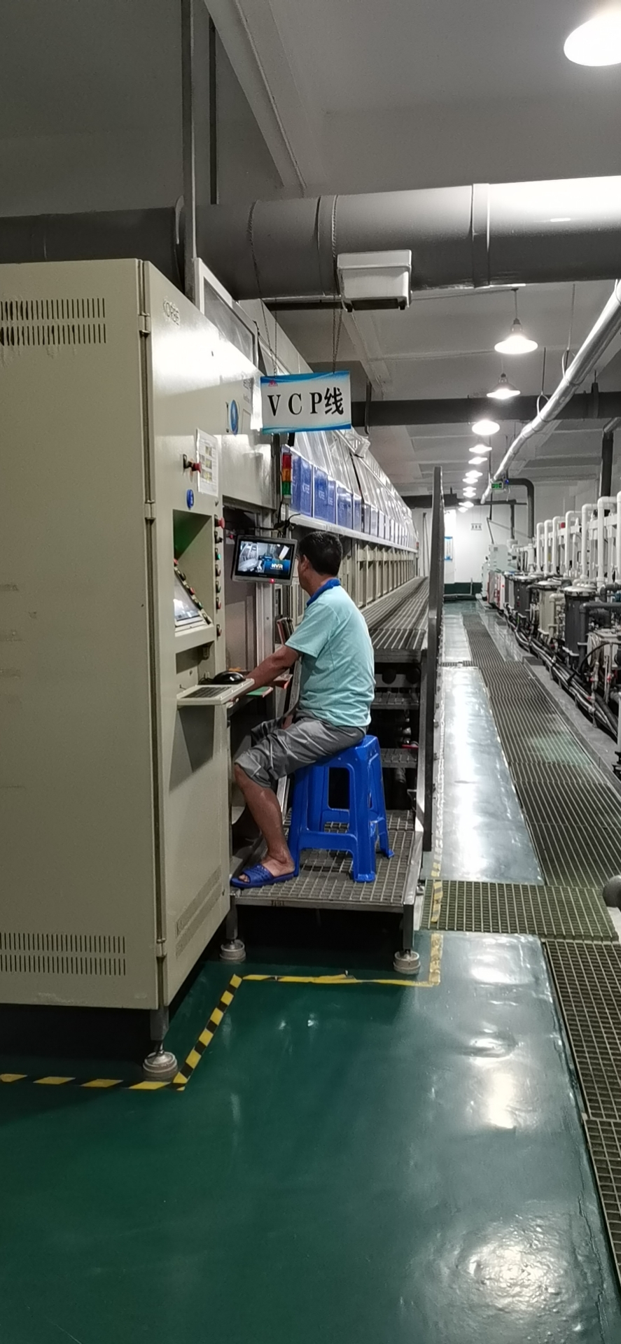
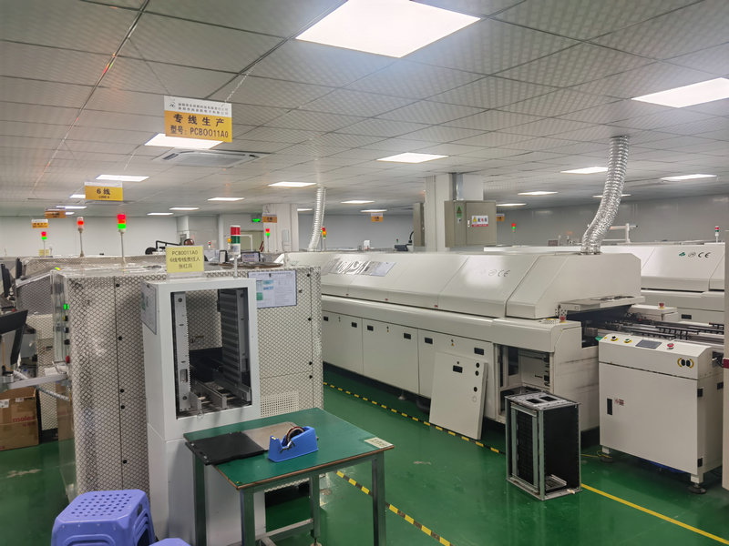
As a Chinese PCB manufacturer, our factory has obtained UL (E358677) and ISO9001:2015 certifications. We use our professional manufacturing and procurement knowledge and experience to help customers reduce operating costs and delivery requirements.
-
Does Haibo accept prototypes or small batch orders?
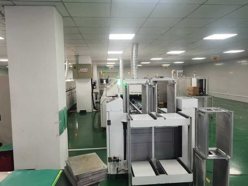
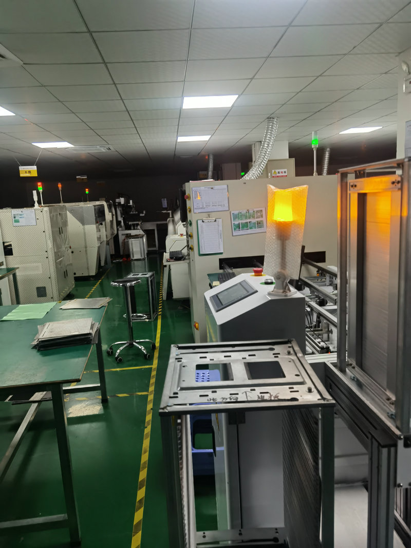
Yes, absolutely so. Since our establishment as a Chinese PCB manufacturer in 2007, we have been focusing on small and medium batch PCB manufacturing and assembly. All of our equipment and personnel are arranged to achieve this goal.
-
Do you offer fast production?
Yes, we are one of the most trusted circuit board suppliers in the fast PCB field, so we are happy to provide our customers with fast production support. The delivery time is as follows:
PCB bare board: 1-3 working days;
Turnkey PCB assembly: 1-2 weeks.
-
Does your PCB comply with RoHS and REACH standards?
Yes, all of our printed circuit boards comply with RoHS and REACH requirements. Please visit www.haibofpcba.cn to view our RoHS and REACH compliance statements.
-
Can you ship the PCB to us?
yes. We can deliver PCBs to your location via express delivery (UPS, FedEx, or DHL), regular air and sea freight. As an experienced PCB board manufacturer, we can ship products to anywhere you want. Please follow this webpage link to learn about our transportation policy:// www.haibofpcba.cn。
-
Can you produce PCBs that meet IPC Level 3 standards?
Yes, as one of the professional PCB manufacturers, we can produce PCBs according to IPC-A-600 Level 3 and assemble PCBs according to IPC-A-610 Level 3.
-
Is Haibo a reliable PCB manufacturer?
of course! Haibo has been engaged in PCB manufacturing business since 2017. It has obtained many international quality certifications, such as ISO9001, ISO13485, UL (E358677), etc. For over a decade, many major global brands have trusted Haibo
-
What is the minimum order quantity for your PCB production?
As a professional supplier of small and medium-sized circuit boards, we do not have a minimum order quantity. We are a printed circuit board manufacturer specializing in sample manufacturing and small to medium batch production. We can produce PCBs from one piece and fully assemble PCBA; For us, no order is too small.
-
Does Haibo provide engineering assistance?
As a Chinese PCB supplier with over 10 years of experience, our engineers evaluate existing designs and assist in optimizing manufacturability (DFM) for new designs, thereby minimizing costs and shortening product time to market.
-
What is the expected delivery cycle for standard production operations?
As a professional PCB manufacturer in China, our average delivery time is as follows:
PCB: 3-10 working days;
PCB assembly: 2-4 weeks;
Complete turnkey electronic assembly: 4-6 weeks.
This depends on the delivery cycle, specifications, and complexity of materials and parts.
-
How long will it take for me to receive a complete quotation?
Our standard delivery cycle for your RFQ is:
PCB bare board: 1 to 2 working days;
Circuit board assembly including component procurement: 1-3 working days;
Complete turnkey box assembly: 3-10 working days.
As an experienced Chinese PCB factory, if you urgently need it, we can also provide you with a quotation within a few hours.
-
What documents are required to produce my printed circuit board?
As a PCB circuit manufacturer, we need PCB files (preferably in Gerber format) that include specifications such as PCB material, circuit board thickness, stacking, copper thickness, surface finish, and the quantity you require.
-
What documents do you need to quote for PCB assembly services?
Electronic circuit board manufacturers like us always require a bill of materials, Gerber data, and quantity forecasts. If you have any questions, please contact us via email: haibo_fpcba1668@163.com .
-
What information do you need to quote for a complete turnkey component?
As a printed circuit board manufacturer, we require your complete data package (including Gerber files, BOM list, assembly instructions, etc.), quantity forecast, and budget. If you have any questions, please contact us via email: haibo_fpcba1668@163.com .
-
How to submit a Request for Quotation (RFQ)?
Please send your inquiry directly to our sales team email: haibo_fpcba1668@163.com
Alternatively, you can visit our sales team page and contact our sales personnel:// www.haibofpcba.cn
-
Is Haibo a Chinese PCB manufacturer?
Yes, Haibo is a Chinese PCB manufacturer. By utilizing advanced electronic component technology and the labor advantage of Shenzhen, China, Haibo supplies high-quality printed circuit boards at low cost.