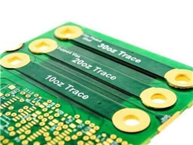
The following are thick copper PCB design specifications for reference.
The minimum line width of thick copper PCB should not be less than 0.3mm.
In general, the minimum distance between adjacent wires used in thick copper PCBs should not be less than 0.25mm.
The distance between the copper foil around the fixed hole used in thick copper circuits and the edge of the hole shall not be less than 0.4mm; There should be no fine lines at a distance of 1.5mm from the edge of the hole.
The distance between high-power heating devices and large volume electrolytic capacitors should be greater than 5mm.
The distance between the wire and the edge of the printed circuit board shall not be less than 3mm, and in special cases not less than 1.5mm, but the wire width must not be less than 1.5mm. The ground wire shall not be less than 0.5mm.
The solder pad must not be connected to the solder pad. Also, do not connect the solder pads to exposed copper foil.
Do high-power components used in heavy copper PCBs have heat dissipation measures.
Have you considered low-density wiring design.
Get a Quotation
Your trusted partner and one-stop supplier for FPC/PCB manufacturing, component procurement, FPC/PCB assembly, and electronic manufacturing. With over 16 years of experience, we have been providing high-quality FPC/PCB at competitive prices to over 1000 customers worldwide. Our company has passed ISO9001:2015 certification and UL certification, and all of our products have undergone 100% electronic testing and passed AOI and X-RAY inspections to meet the highest industry standards. Therefore, please obtain an immediate quote from our sales team as we will handle the remaining matters.


