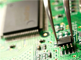
The goal is to achieve zero defects in SMT circuit board assembly. With the continuous pursuit of miniaturization, PCBs are also prone to potential defects, which need to be considered and addressed to achieve higher quality manufacturing. The following are the main defects encountered during the PCB SMT assembly process.
Insufficient solder coverage
Insufficient solder coverage can result in weak and disconnected connections between components and PCB substrate pads. This is usually caused by poor wettability, unoptimized template aperture size, insufficient solder paste amount, and template printing misalignment. Insufficient reflux peak temperature can also lead to this defect.
gravestone
The phenomenon of erecting a monument is a welding defect in which one side of the component is soldered onto the PCB, appearing to be in an upright or vertical position, hence it is called the "monument phenomenon". This defect is caused by incorrect pad design and solder mask application.
Solder bridging
Solder bridging refers to two components that should not be electrically connected coming into contact with conductive solder paste, resulting in a short circuit. Excessive use of solder paste and suboptimal heat distribution can both lead to solder bridging.
Solder Ball
Another common defect encountered during the assembly process of SMT printed circuit boards is solder balls. Solder balls are small spherical solder materials that separate from the joint. As solder balls are conductive materials, they can have adverse effects during electrical testing. Solder balls may be caused by moisture in the solder paste, inaccurate printing, and ineffective solder flux.
Your trusted partner and one-stop supplier for FPC/PCB manufacturing, component procurement, FPC/PCB assembly, and electronic manufacturing. With over 16 years of experience, we have been providing high-quality FPC/PCB at competitive prices to over 1000 customers worldwide. Our company has passed ISO9001:2015 certification and UL certification, and all of our products have undergone 100% electronic testing and passed AOI and X-RAY inspections to meet the highest industry standards. Therefore, please obtain an immediate quote from our sales team as we will handle the remaining matters.
Haibo is an expert in the field of FPC/PCB manufacturing and surface mount assembly in China. Since our establishment in 2017, we have been providing high-quality PCBs to over 1000 customers worldwide. Our factory has passed ISO14001, ISO9001:2015, TS16949, and ISO13485:2016 certifications. We are one of the most trusted small and medium-sized FPC/PCB manufacturers in China.