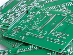
The manufacturing process of single-sided PCB adopts highly automated "printing" and "etching" technologies. The following are the main steps for producing single-sided copper PCB boards:
Schematic diagram and layout
Design is PCB manufacturing The schematic is generated using computer-aided design (CAD) programs. Arrange circuits and components in a schematic using a CAD program that includes tools and elements. Then, the schematic will be transformed into a layout that essentially displays the physical appearance of the printed circuit board.
Application of photoresist
Apply photoresist chemicals (a material sensitive to light or ultraviolet radiation) onto the substrate. A photomask is used to cover parts with copper patterns and expose unwanted copper to ultraviolet light. The exposed part will undergo chemical changes and eventually dissolve.
etch
The uncovered copper is etched away, leaving only the copper required for the design. Etching solution is used to dissolve unwanted copper. Then rinse the circuit board with deionized water to remove chemical residues.
Drilling and electroplating
Use mechanical or laser drilling machines to drill holes on single-sided PCBs. Drills are coated with conductive metal to facilitate contact between components. Holes or through holes come in various sizes, types, and lengths.
Application of solder mask layer
Apply the solder mask layer onto a single-sided copper PCB board through screen printing technology. Solder mask epoxy resin is a thermosetting material that solidifies when heated. Another method is to apply photosensitive film material, then develop and cure it.
Surface Treatment
Hot air solder leveling is a traditional method for surface treatment of copper contact pads. Immerse the exposed single-sided PCB board into the solder bath so that the solder pads can be coated. Another method is to immerse gold through electroless nickel plating, which adopts the electroless nickel plating process and contains flash gold material.
screen print
The printing method of screen printing is almost the same as that of solder mask, which is to apply photosensitive liquid epoxy resin on a single-sided copper PCB and then expose it to ultraviolet light. Another technique is to directly print screen printing ink and then expose it to ultraviolet light for curing.
test
The exposed single-sided PCB board must undergo online testing or flying pin testing during the testing process. ICT is a more effective method as it involves a fixture with a nail bed or spring needle that contacts the test points to determine the electrical response of the circuit board. On the contrary, flying needle testing can flexibly move and access the testing network on the PCB.
Your trusted partner and one-stop supplier for FPC/PCB manufacturing, component procurement, FPC/PCB assembly, and electronic manufacturing. With over 16 years of experience, we have been providing high-quality FPC/PCB at competitive prices to over 1000 customers worldwide. Our company has passed ISO9001:2015 certification and UL certification, and all of our products have undergone 100% electronic testing and passed AOI and X-RAY inspections to meet the highest industry standards. Therefore, please obtain an immediate quote from our sales team as we will handle the remaining matters.
Haibo is an expert in the field of FPC/PCB manufacturing and surface mount assembly in China. Since our establishment in 2017, we have been providing high-quality PCBs to over 1000 customers worldwide. Our factory has passed ISO14001, ISO9001:2015, TS16949, and ISO13485:2016 certifications. We are one of the most trusted small and medium-sized FPC/PCB manufacturers in China.