Layer 1-24
Aron 33N, 35N, 84N, 85N, 86HP 37N, 38N
Rogers AD250C AD350A、CLTE-XT、DiClad 880、827、527
Rogers DT/Duroid 5880, 6002, 6002 RO3003,3005、3010、XNUMX
Passed ISO9001:2015 ISO 13485: 2016 certification and UL certification
Impedance control, back drilling, backplate
Blind and buried holes, 3 N 3 HDI, arbitrary layer HDI
随着对高频和高速电子设备的需求不断增长,对能够完成这些任务的 PCB 的需求变得越来越重要。在一定程度上,特氟龙 PCB 对当前的电子行业产生了影响。这些由聚四氟乙烯 (PTFE) 材料制成的 PCB 将在高性能应用中提供一些独特的优势。本文将提供特氟龙 PCB 板的完整定义、其成分、优点、制造工艺、应用、挑战和未来趋势。
特氟龙是 PTFE(聚四氟乙烯)的品牌名称。这是一种合成含氟聚合物,以其出色的不粘性、热稳定性和耐化学性而闻名。PTFE 因其独特的性能而被广泛应用于电子行业。
特氟龙电路板是采用 PTFE 作为基材的电路板。这是因为它能够处理高频和高速电子应用。PTFE 的低介电常数和低损耗因数使其成为保持信号完整性和最大限度减少高频电路损耗的理想材料。
PTFE层压板是特氟龙电路板的主要成分。它们用玻璃纤维或其他材料增强,以提高其机械性能。特氟龙电路板的主要成分包括:
PTFE层压板: 主要介电材料提供优异的电绝缘性能。
增援: 使用玻璃纤维或其他填料来提高机械强度和尺寸稳定性。
铜箔: 用于创建电路迹线的导电层。
Teflon circuit boards have multiple characteristics that make them suitable for high-performance systems.
Low dielectric constant (Dk): The dielectric constant of PTFE circuit boards ranges from 2.1 ° C to 2.3 ° C, enabling high-speed signal transmission with minimal loss.
Low dispersion factor (Df): The range of loss factor is 0.0003 to 0.001. Low loss factor ensures low signal attenuation and power loss.
High thermal stability: Teflon PCB can withstand temperatures up to 260 ° C, making it suitable for high-temperature applications.
Excellent chemical resistance: They have strong resistance to most chemicals. This will ensure the durability of the PCB in harsh environments.
Low moisture absorption: It can provide stable electrical performance in humid conditions and environments.
Excellent electrical performance: The electrical performance of PTFE PCB boards is excellent, making them very suitable for high-frequency and high-speed applications. The low dielectric constant and dissipation factor of PTFE circuit boards ensure minimal signal loss and distortion while maintaining signal integrity.
High thermal stability: The thermal stability of PTFE PCB enables it to operate reliably in high temperature environments. This characteristic is crucial for applications that generate extreme heat.
Chemical and moisture resistance: Teflon circuit boards have excellent chemical and moisture resistance, which can help them withstand harsh environmental conditions. This is very suitable in industrial environments that come into contact with chemicals and moisture.
Enhanced durability and reliability: The comprehensive electrical performance, high thermal stability, and adaptability to environmental factors make PCB Teflon very durable and reliable. They have a longer lifespan and help reduce the frequency of maintenance and replacement.
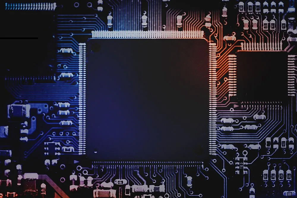
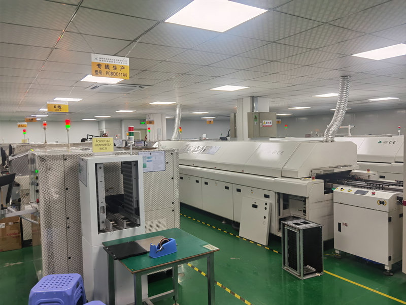
The manufacturing process of PTFE circuit boards involves several specialized steps. This is to ensure that the final product meets high-performance standards. The following provides a detailed introduction to the important stages of the PTFE PCB manufacturing process.
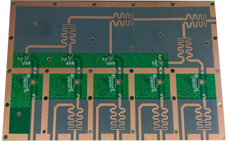
PTFE laminates: Preparing PTFE laminates is the first step. The choice of PTFE sheet depends on the thickness required for manufacturing. To improve mechanical performance, these laminates can be reinforced with fiberglass or other fillers
Copper coating: laminating copper foil onto PTFE board to form a conductive layer of Teflon PCB material. By using high temperature and high pressure to bond copper and PTFE together, a strong bond is formed between the two.
Layer stacking: The stacking of PTFE laminates and copper foils is carried out in the required order. In order to obtain an accurate final PCB, it is necessary to align each layer correctly.
Compression and curing: Stacked layers are subjected to high pressure and high temperature. This process fully solidifies the PTFE resin, forming a sturdy multi-layer laminated board. By maintaining compression parameters such as temperature, pressure, and time, PTFE resin can be fully cured.
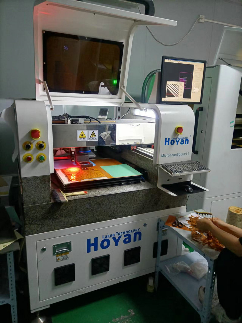
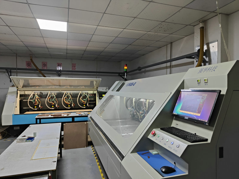
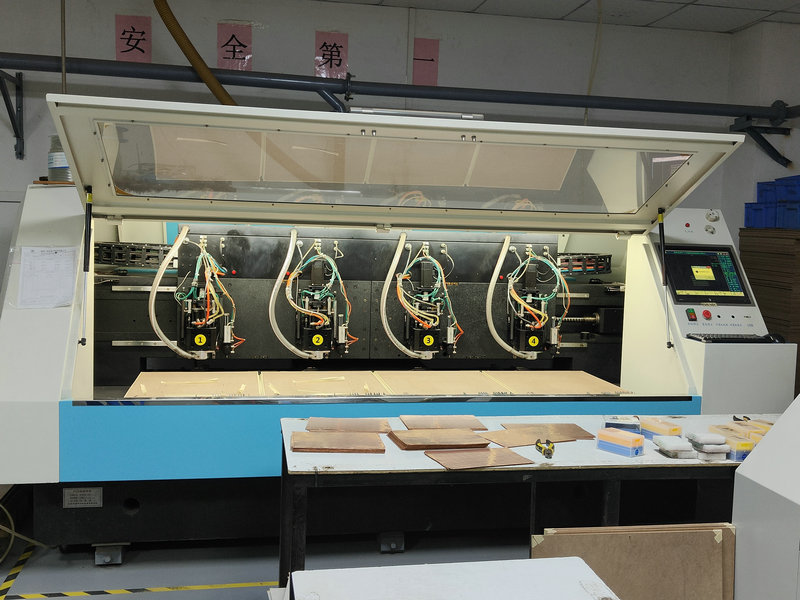
Drilling: Drilling is to create through holes and points for installing components. The drilling of PTFE materials requires specialized equipment and techniques to prevent issues such as stains or burrs.
Chemical copper plating: Complete this operation to create conductive pathways between different layers of the PCB. This is achieved using the chemical copper plating process. Depositing a thin layer of copper on the hole wall is crucial for establishing electrical connections in PTFE circuit boards.
Applying photoresist: A layer of photoresist is applied on the surface of a copper-clad laminate to determine the circuit pattern of a PTFE circuit board.
Apply solder mask layer: Apply a solder mask layer on the PCB to protect copper traces from oxidation. It is also used to prevent welding bridges when welding components. To ensure that the final product maintains its high-performance characteristics, a solder mask compatible with Teflon was used.
UV exposure and development: The applied solder mask is exposed to ultraviolet light through a photomask, which defines the mask area that needs to be removed. Then develop the exposed area, leaving only the required solder mask layer.
For exposed copper areas, surface treatment should be applied to enhance solderability and protect copper from oxidation. Some common surface treatments used in the manufacturing of Teflon circuit boards include:
Chemical nickel gold plating (ENIG)
Organic Solderability Protection (OSP)
Tin immersion or silver immersion
Parts assembly
Welding: Assemble the components onto the PCB using a welding process that perfectly matches the PTFE material. To ensure consistent connection, specialized welding techniques were used.
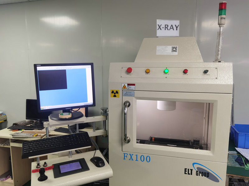
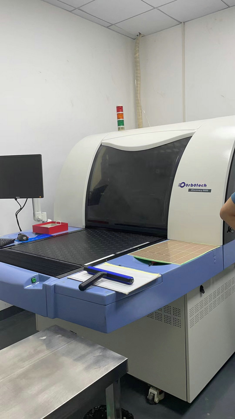
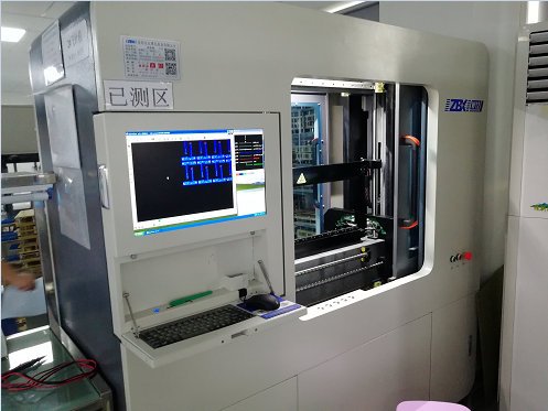
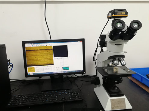
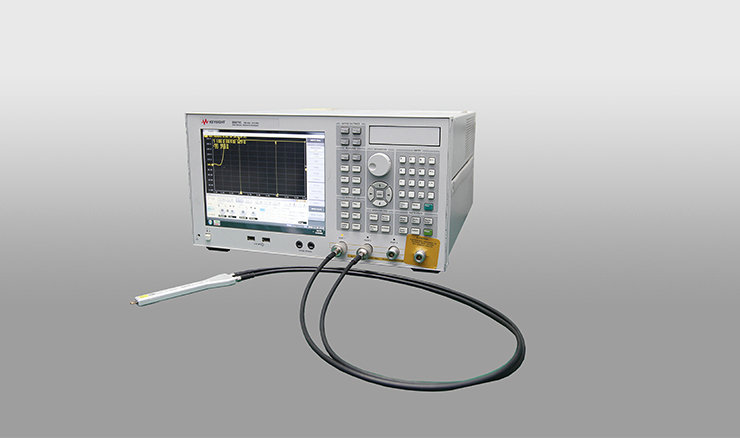
There is a test conducted to ensure the quality of the manufactured PCB. The testing conducted by PTFE PCB suppliers includes:
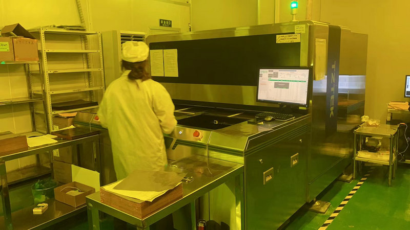
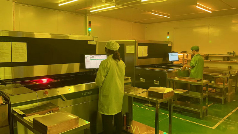
Electrical inspection: Conduct electrical testing to ensure that all connections are fault free and free from short circuits or open circuits.
Vision examination: Check for any physical defects or damages, such as incomplete solder joints, solder bridges, or misaligned components.
Functional testing: Ensure that the PCB achieves the expected performance in the expected application. This is done on the PCB in a simulated or actual operating environment.
Teflon circuit boards are widely used in various high-performance applications, where electrical performance and reliability are crucial. Below are some key applications listed.
Teflon circuit boards are most suitable for high-frequency RF and microwave circuits in the telecommunications field. They will ensure minimal signal loss and distortion, which will help maintain the integrity of high-frequency signals. Teflon PCB board manufacturers also produce PCBs for aviation electronics and radar systems due to their high thermal stability and reliability.
Due to its high-frequency performance, PTFE PCB can be applied to ADAS (Advanced Driver Assistance Systems). ADAS systems require precise signal processing and minimal signal loss. Due to their high thermal stability, they can also be used for ECU (Engine Control Unit). This feature makes them suitable for ECU operation in high-temperature environments of automotive engines.
Teflon circuit boards are used for measuring equipment and for testing purposes. The low signal loss and excellent performance of PTFE circuit boards are crucial for precise measurement in high-frequency applications. Teflon PCB boards are widely used in the field of automation and control systems. This is mainly because these PCBs have durability and adaptability to harsh environments.
Teflon PCB is used for diagnostic and imaging equipment such as MRI and CT scanners. These devices require PCBs that can generate high output to accurately process high-frequency signals. Teflon circuit boards are also used in implantable medical devices due to their biocompatibility and reliability. Devices using this PCB will operate reliably and for a long time inside the human body.
Teflon PCBs are widely used in high-tech electronic devices, especially in the telecommunications industry. However, due to its unique material properties, there are some challenges in production. Only experienced manufacturers can provide high-quality PCBs made of PTFE materials.
Problems in material processing and handling.
Difficulty in drilling and processing.
The material cost is relatively high.
The complexity of the manufacturing process.
Design challenge.
Challenges in thermal management.
The issue of maintaining signal integrity for high-frequency applications.
If pursuing cost-effective FPC manufacturing services, choosing a Chinese manufacturer is the best choice. As a manufacturing powerhouse, China has abundant resources, cheap labor, and a large number of technical personnel. We recommend Haibo, a Chinese FPC assembly service provider with over 10 years of experience, who has performed outstandingly in various aspects
Efficient and reasonable quotation:There is an efficient quotation process to assist you in making decisions, providing reasonable prices and highly competitive quotes in China.
High quality and reliable products:Produce high standard printed circuit boards, manufacture and test according to specifications, international standards, and internal controls, and conduct pre production inspections to ensure robust processes.
Quick and on-time delivery:The assembly equipment is in good condition, with high productivity, minimal downtime, short delivery time, and also provides urgent services.
Timely and effective response:Always respond to customer needs, provide accurate information, answer questions through multiple channels, and offer one-stop services.
Strong technical strength:China's FPC manufacturing technology is leading, and Haibo has a complete SMT solution that covers assembly, inspection, and other capabilities. It also provides prototype production and customization services.
mobile phone: 86-15113315665
Contact: Chen Changhai
mobile phone: 86-18676922028
E-mall: haibo_fpcba1668@163.com
Address: 3rd Floor, Building 2, Fuxing Industrial Park, Building B, Chuangye 1st Road, Jiangbian Community, Songgang Street, Bao'an District, Shenzhen