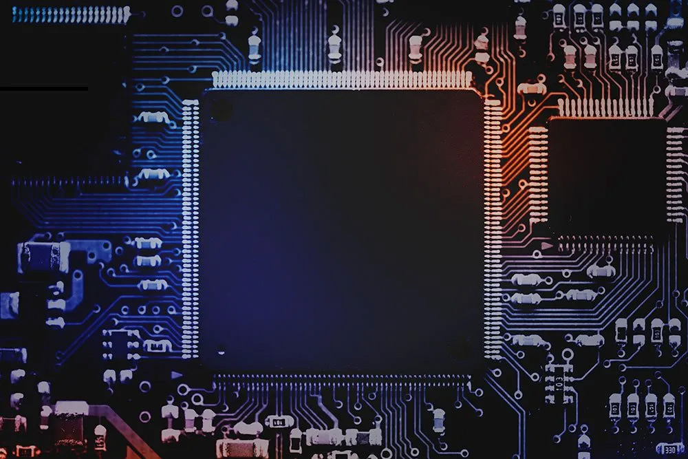
1-40 layer mass production&100 layer prototype
FR4、 High speed, microwave and radio frequency, metal core, ceramic PTFE
Blind and buried holes, stacked and staggered holes, arbitrary layer HDI
Blockage of conductive and non-conductive vias
Backdrill, Backboard, Embedded Device, IC Carrier Board
ISO9001: 2015 certification and UL certification
无论你走到哪里,你都会发现至少有一种电子设备可以简化困难的任务。最接近的例子是家用电器,如吸尘器、洗衣机、冰箱和电视。这些设备中的大多数现在都被标记为“智能”,因为它们可以非常高效地自动运行。电子设备的内部系统由刚性印刷电路板 (PCB) 组成,可执行从基本到复杂的功能。当今制造的大多数 PCB 仍由刚性 PCB 制成。我们将了解有关刚性印刷电路板的更多信息。
Rigid PCB is a printed circuit board made of solid substrate material, which once manufactured, cannot bend or deform, and cannot be changed. Rigid printed circuit board is a traditional type of PCB widely used in automotive, commercial, and industrial fields. The most famous and best-selling type of rigid PCB substrate or laminate on the market is FR4, which is a flame-retardant epoxy woven glass fiber. FR4 has advantages such as high hardness, good dielectric properties, and good thermal performance. The choice of rigid PCB laminate material depends on the expected application. Some applications may require specific materials with low thermal expansion coefficients or different dielectric constants.
A rigid PCB board can be divided into three main layers: insulation substrate, copper film, and photoresist layer. The insulating substrate is the FR4 mentioned earlier. The copper layer is etched to form a conductive path and realize the conductive part of the circuit. The thicker the copper layer, the better the current carrying capacity. The photoresist layer is a protective material that covers the copper layer. Rigid printed circuit boards can also be classified based on the number of layers: single-sided, bidirectional, and multi-layer rigid printed circuit boards have more layers, higher functionality, and more complex manufacturing processes.
Flexible printed circuit boards are more suitable for devices with limited space, while rigid printed circuit boards have better mechanical structures and are more durable than flexible PCBs because they are less prone to expansion and have good mechanical strength.
Rigid PCB boards allow for multi-layer structures and connection density, which means circuit board designs have higher functionality and flexibility.
Rigid PCB board, as the earliest technology in printed circuit boards, has become very mature and developed. Its production process is very efficient, automated, and standardized.
Due to the high reliability of rigid printed circuit boards, most applications still rely on their use. Rigid printed circuit boards are not easily deformed due to their structural rigidity and durability.
Rigid PCBs have a wide range of applications, including consumer electronics, automotive, military, industrial, and medical applications. Here are some known applications of rigid PCBs.
Computer motherboard
storage device
Communication technologies such as satellites, radio, and antennas
mobile phone
medical equipment
Vehicle infotainment system
Industrial electronic products such as control systems and instruments
Firstly, the design of a rigid printed circuit board must be generated by drawing circuits in computer-aided design software. The schematic uses pin references for each connection to assign each component to a rigid printed circuit board. Then proceed with PCB layout to display the final physical appearance of the rigid circuit board.
In the lamination process, the prepreg is laminated with copper foil at high temperature and high pressure. The prepreg is composed of uncured resin, and during the lamination process, high temperatures can cause the resin to become viscous and eventually cure. This process is carried out in a closed hot press machine.
The application of photoresist is an essential step in the manufacturing of rigid PCBs, in order to form a protective layer on the easily oxidizable copper layer. During this process, positive photoresist is a widely used technique, in which the portion of photoresist exposed to ultraviolet light becomes highly soluble in developer chemicals. Some commonly used developer solutions are sodium hydroxide or alkaline solutions.
The next step in producing rigid PCBs is to etch away unwanted copper patterns using etchants such as ferric chloride and ammonium chloride. In order to obtain consistent and high-quality copper patterns, it is necessary to specify and control the etching rate and etching solution concentration. Etching can be carried out through immersion, spray etching, or sputtering methods. After the etching process, there is a rinsing step to clean the remaining photoresist.
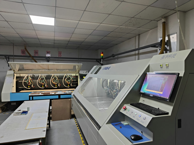
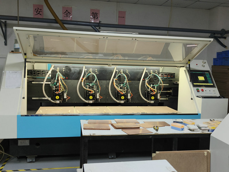
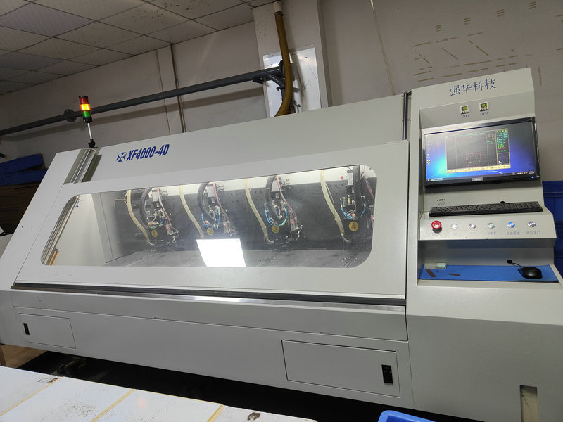
Use a computer programmable drilling machine to drill and conduct holes. Small electronic components require drill bits with smaller diameters. For fiberglass rigid PCBs, diamond tungsten carbide drill bits are being used. Accurate drilling must be achieved by optimizing drilling speed, force, and geometry. Usually, boards are stacked together to drill holes simultaneously. There are various types of drilling techniques, such as laser, micro drilling, and micro machining.
Solder mask, also known as "solder mask", is applied to rigid printed circuit boards. Welding masks are used as protective coatings to isolate conductive and insulating surfaces on rigid PCBs. The photolithography process can be performed using liquid photosensitive imageable solder mask (LPSM) by exposing the photosensitive solder resist to ultraviolet light for curing. Epoxy liquid can also be directly screen printed onto rigid printed circuit boards and thermally cured.
The exposed copper part undergoes surface treatment process. Please remember that copper is easily oxidized when exposed to the environment. Although copper is susceptible to corrosion, it remains the preferred basic conductive material due to its excellent thermal and electrical conductivity. Due to the possibility of oxidation during subsequent heat treatment during assembly, surface treatment is required on the exposed solder pads.
Surface treatment ensures effective welding of components. Some surface treatment options include hot air solder leveling (HASL) and electroless nickel immersion gold (ENIG). HASL coats copper with a layer of solder, while ENIG involves nickel and gold plating to ensure good connectivity.
In order to print information on rigid PCBs, screen printing technology is required. PCB information, such as component codes, pin locators, company logos, reference points, regulatory marks, and other traceability labels, can be screen printed on rigid PCBs. There are multiple methods to apply screen printing information to rigid PCBs. One method is to use templates and scrapers to transfer ink patterns onto rigid PCBs. Another method is liquid light imaging (LPI), which is more suitable for high-density rigid printed circuit boards. This method uses photosensitive ink, which is then developed and cured to produce screen printing.
If pursuing cost-effective FPC manufacturing services, choosing a Chinese manufacturer is the best choice. As a manufacturing powerhouse, China has abundant resources, cheap labor, and a large number of technical personnel. We recommend Haibo, a Chinese FPC assembly service provider with over 10 years of experience, who has performed outstandingly in various aspects
Efficient and reasonable quotation:There is an efficient quotation process to assist you in making decisions, providing reasonable prices and highly competitive quotes in China.
High quality and reliable products:Produce high standard printed circuit boards, manufacture and test according to specifications, international standards, and internal controls, and conduct pre production inspections to ensure robust processes.
Quick and on-time delivery:The assembly equipment is in good condition, with high productivity, minimal downtime, short delivery time, and also provides urgent services.
Timely and effective response:Always respond to customer needs, provide accurate information, answer questions through multiple channels, and offer one-stop services.
Strong technical strength:China's FPC manufacturing technology is leading, and Haibo has a complete SMT solution that covers assembly, inspection, and other capabilities. It also provides prototype production and customization services.
mobile phone: 86-15113315665
Contact: Chen Changhai
mobile phone: 86-18676922028
E-mall: haibo_fpcba1668@163.com
Address: 3rd Floor, Building 2, Fuxing Industrial Park, Building B, Chuangye 1st Road, Jiangbian Community, Songgang Street, Bao'an District, Shenzhen