Rigid, flexible, rigid flexible combination HDI、 High TG, high speed, high frequency, backplane, embedded PCB, IC carrier board
4-40 layer mass production and up to 100 layer prototype
Blind and buried holes, graded and staggered holes, back drilling
Conductive and non-conductive vias are blocked, VIPPO
ISO9001: 2015 certification and UL certification
100% electronic testing, AOI testing, and visual inspection
众所周知,电子和半导体公司在市场上发展迅速。过去,人们使用手机,但它们只能拨打和接听电话。现在技术已经发生了变化,由于使用多层 PCB 板,移动手机已经更新了更多应用。它们很容易安装在手机的许多 SMD 和 DIP 部件上,以获得有效的解决方案。因此,越来越多的电子设备使用多层电路板来实现复杂尺寸的更多功能。
多层 PCB 是一种具有两层以上铜层的印刷电路板。与 单 和 双层PCB 多层印刷电路板通常只有一层或两层铜箔,而多层印刷电路板通常有4至18层,在特殊应用中甚至可达100层。
多层电路板中,外层定义为顶层和底层,PCB上安装许多SMD和Dip封装,以实现多种功能。除了顶层和底层外,还有许多内层,内层定义为信号层、电源地层和平面层。所有这些层都通过通孔钻连接起来,甚至通过盲孔和埋孔来实现复杂的电子连接。
外层和内层通过介电芯和预浸料粘合在一起。因此,这种结构看起来像是内层、介电芯和预浸料的三明治。从下图可以看出,您可以更清楚地了解多层印刷电路板及其连接方法。此外,您可以看到内层位于介电预浸料和芯上。
核心: 多层电路板的核心是传导电信号和提供电源分配的导电铜层。
预浸料: 多层电路板的预浸料是PCB堆叠中连接芯线与芯线、芯线与层的绝缘材料。
铜箔: 铜箔是应用于电路板内层和外层的初始铜厚度。 多层板 板。
阻焊层: 阻焊膜是一种保护膜,用于保护多层电路板上的元件免受氧化、腐蚀、污染等外部环境因素的影响。
表面处理: 表面处理是多层 PCB制造 对露铜进行最终处理,防止短路、断路、氧化等问题。
过孔: 过孔是多层电路板上用于不同层之间电气连接的孔,包括通孔、盲孔、埋孔和背钻孔。
Through hole drilling (including through holes): Through hole drilling or through holes means that all boreholes are connected from top to bottom to each layer.
Blind hole: Blind hole refers to the connection between the top or bottom layer and the inner layer through a through-hole, as shown in the following figure.
Buried hole: Buried hole refers to all through holes connected to the inner layer. The buried hole will never connect to the outer layer.
Stacked via: Stacked via is defined as a through-hole connected in a straight line from the outer layer to the inner layer for the easiest wiring and correct electrical connection.
Interlocking via: Interlocking via refers to a via that is not connected to adjacent layers in a straight line. Its connection with adjacent layers has a certain angle, as shown in Figure 2.
Micro pores: Micro pores are pores smaller than 0.15 millimeters. Stacking and interleaving are both micro vias, which generally exist on HDI multi-layer PCBs.
The main advantage of multi-layer PCB boards is that they can install more components and functions in a smaller area. Electronic components are becoming smaller and smaller, so we can reduce the size of PCBs with powerful functions. PCB designers set wiring and component placement according to PCB design rules, so using multiple layers can easily minimize PCB size. It allows for the installation of many components on the same board to provide higher part density. In addition, compared to simple circuit boards, these circuit boards have many functions and uses. Here are some of the main advantages of multi-layer circuit boards.
Minimize PCB size: We can use the inner layer to reduce the size of multi-layer PCB boards according to PCB design rules.
High component density: Multilayer PCB boards have high component density.
More features: Due to the increasing number of wires and drill holes placed on multi-layer PCBs, more electronic component connections are needed to achieve more functionality.
Powerful performance: We can place high-power components to achieve powerful performance.
High thermal conductivity: Multilayer PCB boards have high thermal conductivity.
High mechanical strength: It provides mechanical strength. Therefore, we can easily transport heavy components.
More programs: For multi-layer PCB boards, the manufacturing process is very lengthy. Therefore, we need more processes to handle them.
Higher cost: The production cost of multi-layer boards is very high, sometimes due to the need for special processes, the cost can be even higher. If any problems arise, rework is required to solve them, which requires more time and money.
Long manufacturing time: It takes a long time to manufacture them. (For reference only: Some manufacturers have more machines, so the time required to manufacture them is shorter.)
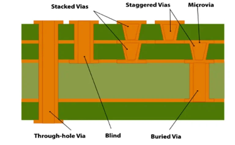
According to special requirements, multi-layer PCB production requires many special processes, such as edge plating, hole stacking, hole filling and plugging, blind buried holes, etc. Here we only discuss the typical multi-layer circuit board production process.
DFM check: In this verification check, DFM engineers will verify all layers. He will verify all error types in the PCB. Therefore, the production workshop can easily produce circuit boards without any errors.
Material selection and cutting: There are many materials to choose from in the production inventory. Therefore, select and cut materials according to the order requirements.
Inner layer process: At this stage, UV film and dry film are used to transfer the inner layer image onto the printed circuit board, followed by etching. During the etching process, unwanted copper in the inner layer is removed.
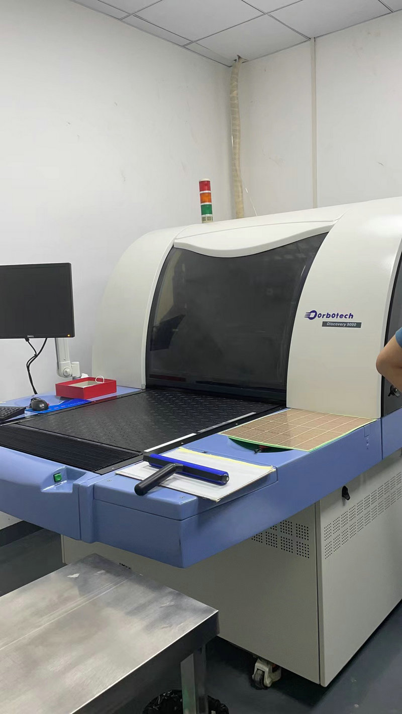
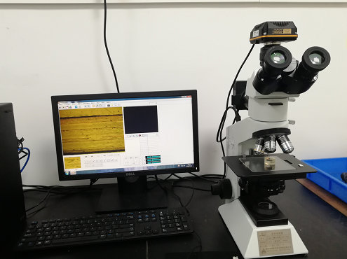
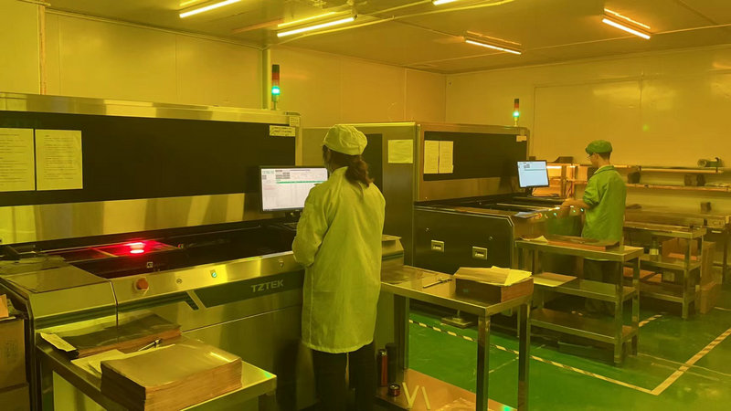
AOI: AOI stands for Automatic Optical Inspection. Therefore, this detection converts the circuit image into a digital image. In addition, AOI will inspect the circuit board to ensure that it has no defects. Then, the manual visual inspector will manually verify the inner layer. This is beneficial for all of us because if any malfunctions enter this stage, they will be controlled and resolved.
Lamination: lamination is the process of combining or bonding inner copper foil, core board, and prepreg to form a solid layer. The laminating machine sets some parameters to heat and pressurize these inner layers to form solid layers.
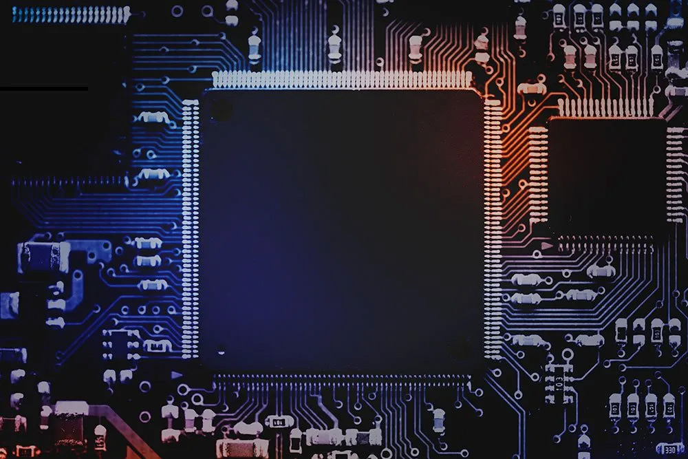
Drilling: There are various drilling methods for multi-layer printed circuit boards according to requirements, such as blind buried holes. Therefore, the drilling machine drills the circuit board based on the given data input into the drilling machine.
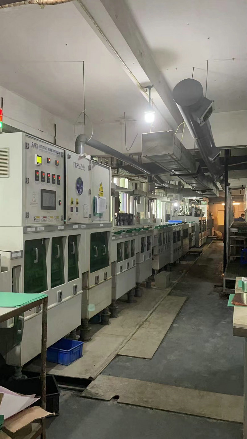
Copper plating: Place the PCB into a copper plating groove and add a copper plating layer on the PCB. This will increase the thickness and make the PCB more robust.
Outer layer process: This process is the same as the inner layer. However, the inner layer is expanded as needed, while the outer layer only has two layers, namely the top layer and the bottom layer. In addition, the top and bottom layers are completed through image transfer and etching. Therefore, other processes are free of charge.
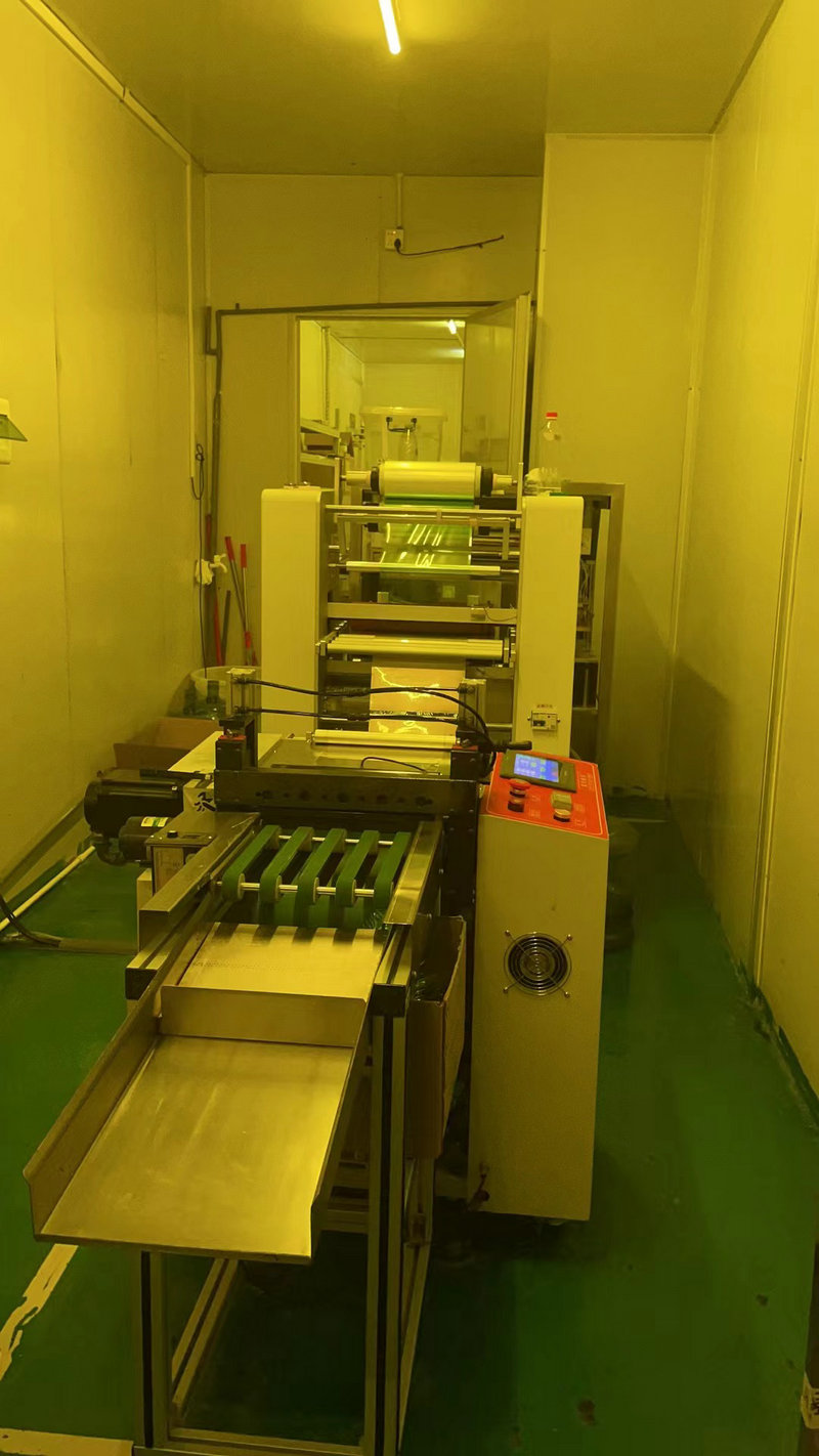
Masking and legend printing: After the copper layer is correctly completed, apply the solder mask layer and screen printing layer to the PCB. Solder mask pads are used to solder parts on PCBs and screen printed layers, as indicated in reference designs, part orientations, part numbers, and company logs.
Surface treatment: Surface treatment of PCB according to customer requirements. PCB surface treatment can improve testing capabilities and provide connections between copper and solderable components.
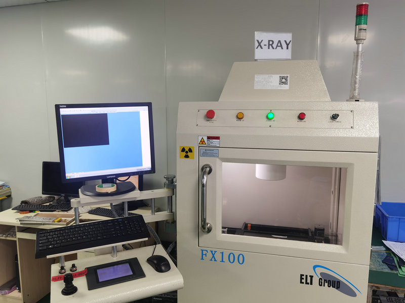
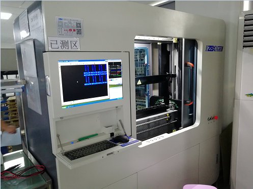
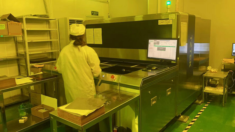
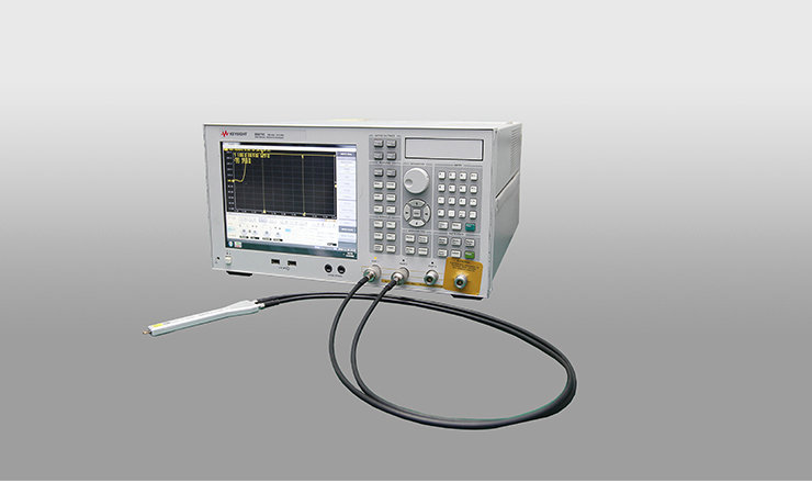
Electrical testing: At this stage, all connections are verified by an electrical testing machine. Therefore, we know that any short circuit or open circuit can be easily found through this electrical test. Flying needles are the best method for verifying electrical testing.
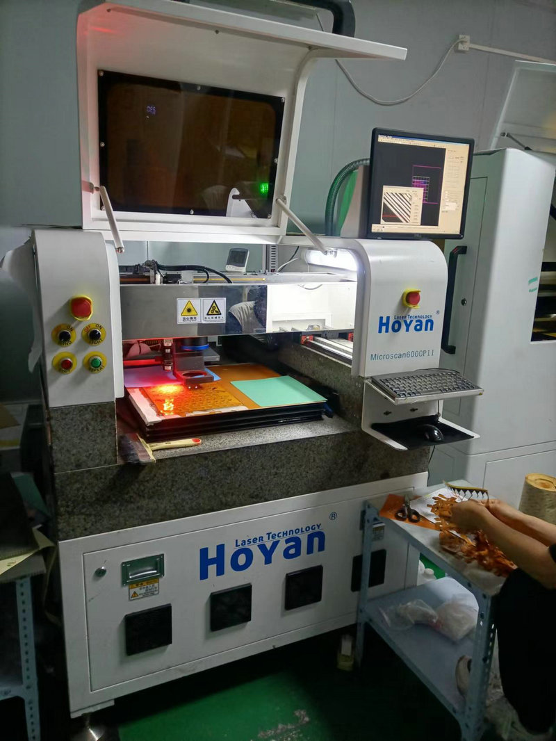
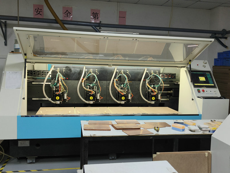
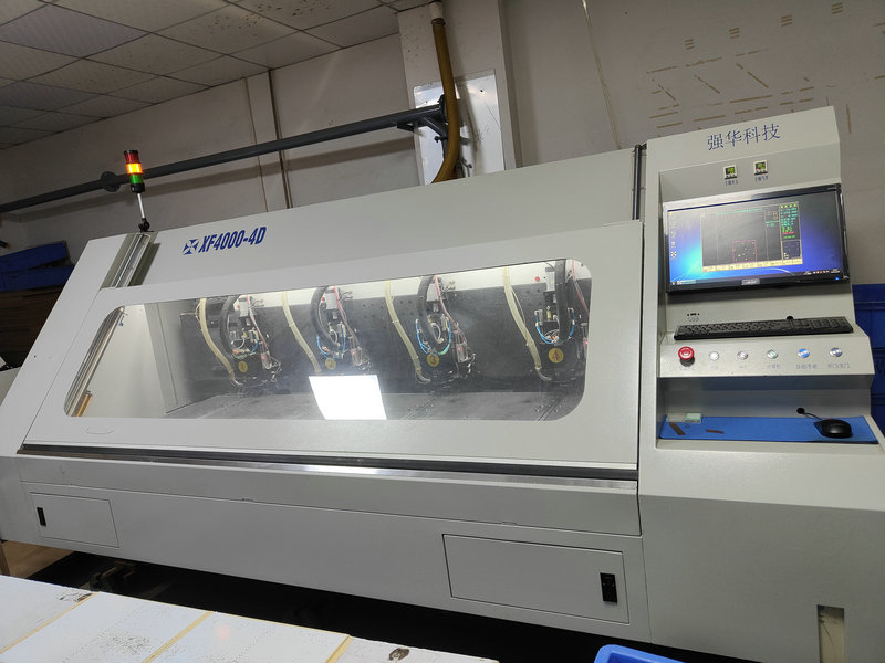
Routing and rating: PCBs come in various shapes. Therefore, irregular plates mainly need to be milled and retained to separate the plates. And rectangular plates need to be carved to divide them. In most cases, these processes are carried out according to customer requirements and company standards.
Final inspection and packaging: After the entire production process is completed, the circuit board will be sent to the inspection team, which will verify whether the PCB is made correctly. Then, the PCB will be shipped to the corresponding address along with the packing list and bubble wrap.
If pursuing cost-effective FPC manufacturing services, choosing a Chinese manufacturer is the best choice. As a manufacturing powerhouse, China has abundant resources, cheap labor, and a large number of technical personnel. We recommend Haibo, a Chinese FPC assembly service provider with over 10 years of experience, who has performed outstandingly in various aspects
Efficient and reasonable quotation:There is an efficient quotation process to assist you in making decisions, providing reasonable prices and highly competitive quotes in China.
High quality and reliable products:Produce high standard printed circuit boards, manufacture and test according to specifications, international standards, and internal controls, and conduct pre production inspections to ensure robust processes.
Quick and on-time delivery:The assembly equipment is in good condition, with high productivity, minimal downtime, short delivery time, and also provides urgent services.
Timely and effective response:Always respond to customer needs, provide accurate information, answer questions through multiple channels, and offer one-stop services.
Strong technical strength:China's FPC manufacturing technology is leading, and Haibo has a complete SMT solution that covers assembly, inspection, and other capabilities. It also provides prototype production and customization services.
mobile phone: 86-15113315665
Contact: Chen Changhai
mobile phone: 86-18676922028
E-mall: haibo_fpcba1668@163.com
Address: 3rd Floor, Building 2, Fuxing Industrial Park, Building B, Chuangye 1st Road, Jiangbian Community, Songgang Street, Bao'an District, Shenzhen