Rigid HDI and rigid flex combination HDI
i N i (i≥2) HDI, Any layer HDI
Blind and buried holes, stacked holes, and staggered holes
Blockage of conductive and non-conductive vias
Minimum 1.5/1.5 mil line width/spacing
Backdrill, Backboard, Embedded Device, IC Carrier Board
HDI PCB 的全名是高密度互连印刷电路板。这意味着 PCB 具有更小的走线、钻孔和更多封装在该空间中的元件。连接元件和 IC 的走线非常细,载流也非常低。该技术采用微孔、盲孔和埋孔代替传统的通孔。这有助于封装更多元件并有效利用空间进行布线和其他用途。随着计算机的普及,过去 4 年来高密度 PCB 板的使用量不断增加。高密度互连 PCB 需要遵守以下 IPC 标准:IPC - 2315、IPC - 2226、IPC - 4104 和 IPC - 6016。
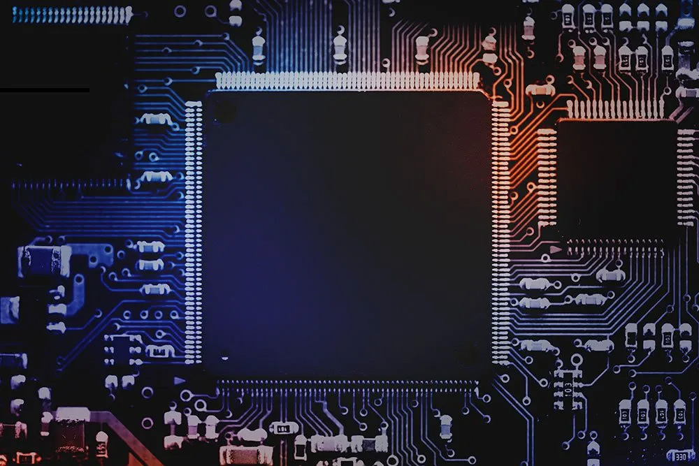
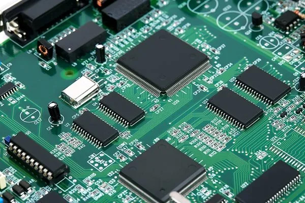
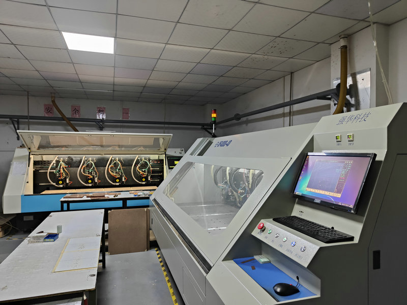
HDI PCB has the following main characteristics: high number of layers, small line width and spacing, small via holes such as blind holes and buried holes, several rounds of stacking and lamination. Here is the detailed information:
Due to the fact that HDI circuit boards are typically designed with very complex functions within a compact PCB area, many traces and connections need to be dispersed across multiple layers. Typically, HDI circuit boards should have at least 4 layers, while most high-density interconnect PCBs range from 6 to 12 layers.
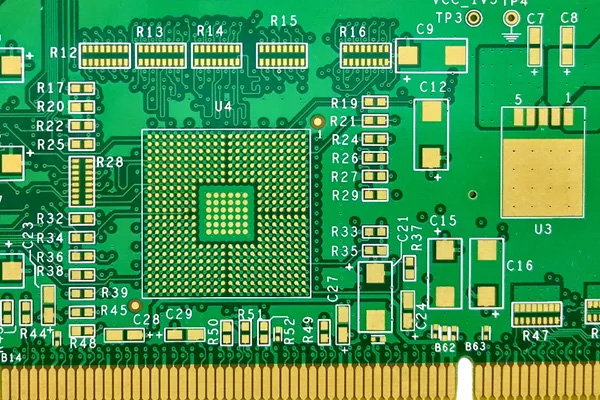
Due to the need to lay a large number of traces in a very small space, the width and spacing of the traces obviously need to be designed as small as possible. Therefore, the routing width and spacing of most high-density interconnect PCBs are as small as 4 mil or less. In some designs, the wire width and spacing are 2mil, which is very difficult in PCB production.
HDI circuit boards require smaller through holes, with drill holes less than 6 mil, so the through holes need to be stacked and micro through holes set between layers. The standard practice is that micro vias are usually filled or plated. High density interconnect PCBs require more wiring area, so VIP technology is used to increase density. This technology is used in conjunction with micro vias inside solder pads, and the wiring connecting them is very small, providing a larger breakthrough area for wiring. According to the placement position of the through-hole on the solder pad, the types include embedded, partial, and offset center solder pad through-hole, as shown in the following figure.
High density interconnect PCBs use various types of through holes based on layer stacking, and the construction of through holes plays a crucial role. Micro through holes, blind through holes, and buried holes are types of through holes used to replace through holes. Metalization is a process that ensures that there are no gaps in the through holes during the stacking process. The pattern of stacked through holes also plays a crucial role in achieving low aspect ratios. The core of high-density interconnect PCBs is thicker than other substrate layers, so using traditional buried holes can help with auxiliary connection applications.
Micro through-hole: Micro pores refer to holes with a diameter less than 0.15mm (6mils).
Blind hole: A blind hole is a hole drilled from the top or bottom layer to the inner layer, with only one side of the hole visible.
Burial hole: Burial hole is a hole buried in the middle layer, which we cannot see from the side of the PCB.
Interlocking through holes: Stacking staggered through holes is a gradual arrangement of micro through holes.
Stacked through holes: Stacked through holes are formed by stacking micro through holes in each layer.
High density interconnect PCBs use various types of through holes based on layer stacking, and the construction of through holes plays a crucial role. Micro through holes, blind through holes, and buried holes are types of through holes used to replace through holes. Metalization is a process that ensures that there are no gaps in the through holes during the stacking process. The pattern of stacked through holes also plays a crucial role in achieving low aspect ratios. The core of high-density interconnect PCBs is thicker than other substrate layers, so using traditional buried holes can help with auxiliary connection applications.
Micro through-hole: Micro pores refer to holes with a diameter less than 0.15mm (6mils).
Blind hole: A blind hole is a hole drilled from the top or bottom layer to the inner layer, with only one side of the hole visible.
Burial hole: Burial hole is a hole buried in the middle layer, which we cannot see from the side of the PCB.
Interlocking through holes: Stacking staggered through holes is a gradual arrangement of micro through holes.
Stacked through-hole: Stacked through-hole is a micro through-hole in
Each layer is stacked on top of each other.
Similar to the standard PCB structure, stacking is constructed layer by layer. The main change is the ability to use multiple rounds of stacking and lamination to achieve multiple blind burial designs. In addition, in high-density interconnect PCBs, there are high-density traces and thin dielectric layers mirrored on the thick core layer.
Place a negative photoresist film and then use ferric chloride to etch away the non-conductive portion of the trace, leaving behind the conductive portion.
Then wash off the photoresistor film with a chemical solution.
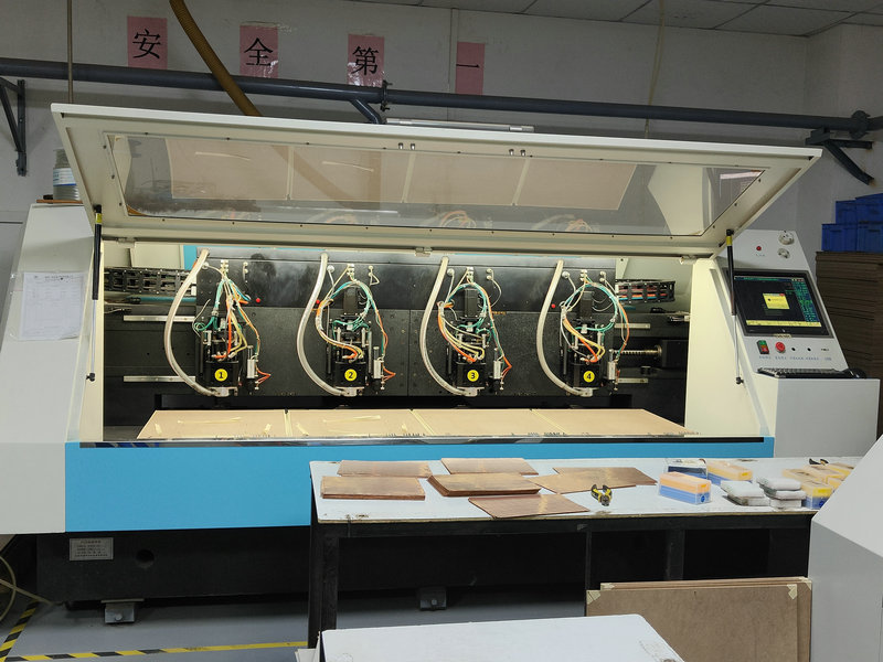
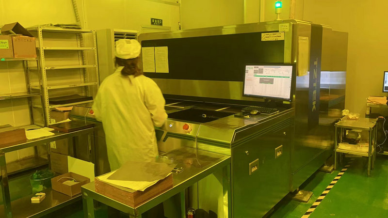
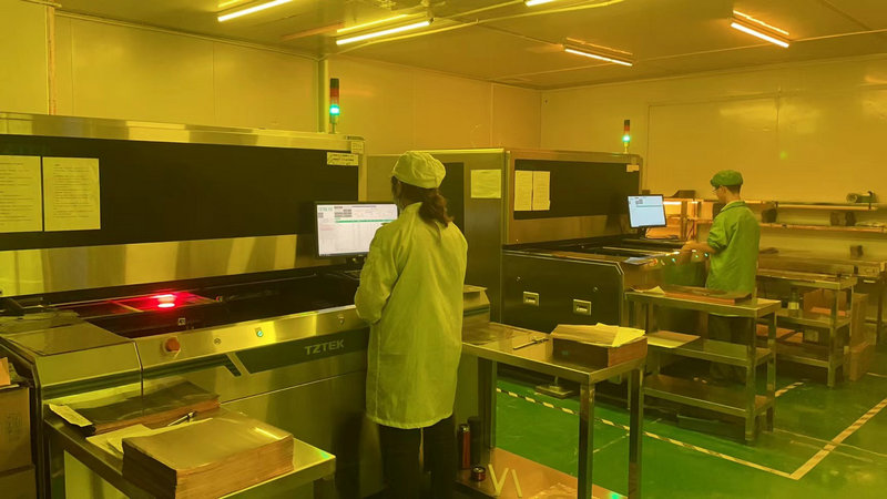
Through holes are drilled using mechanical or laser drilling methods, while chemical processes are used for high-density areas.
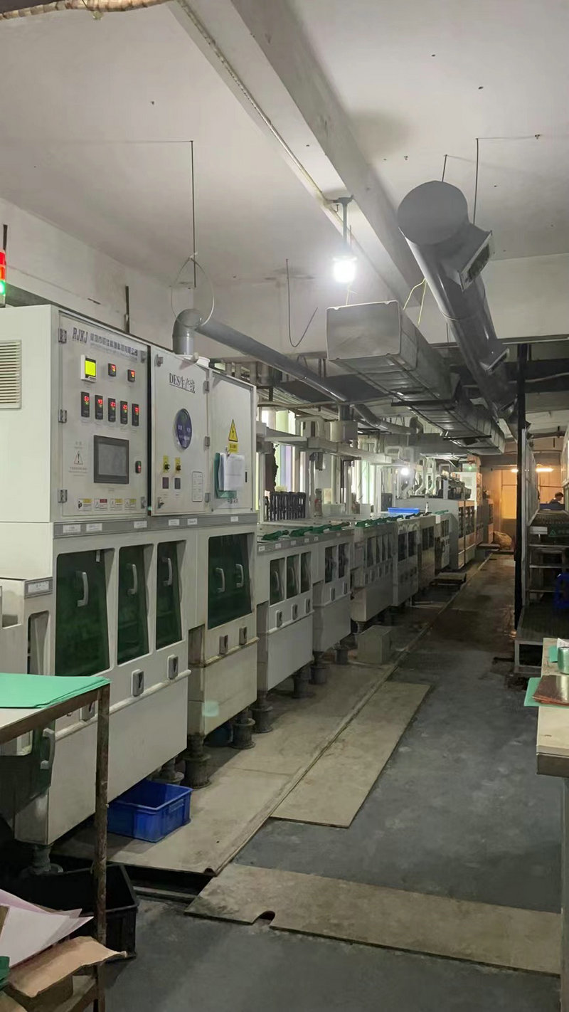
Internal interconnection is formed through metallization process.
Repeat the stacking process to obtain outer layer stacking and the required electroplating process.
High density interconnect PCBs are used daily for various complex system based applications, such as personal computers, mobile phones, tablets, cameras, and supercomputer systems like space stations.
Size and weight: Due to the space occupied design and complexity of the circuit board, compact size and lightweight are the main advantages, which retain the functional features of the overall situation. Low cost: Manufacturing costs may seem high, but when the entire standard PCB design is considered from a component and size perspective, this can reduce the cost of the entire application several times. Performance and reliability: HDI circuit boards offer higher performance with less noise and signal integrity issues. Although the component packaging is small and the spacing is also small, the performance of HDI is still reliable. The use of micro through holes and buried holes instead of through holes can provide greater advantages for high-density interconnect boards. The smaller size with aspect ratio provides additional advantages. Through hole pad technology provides higher signal integrity while reducing signal path length. Time to market: The production process of high-density interconnect PCBs exhibits excellent performance, enabling production and testing of compact applications in less time.Automotive applications and subsystems: High density interconnect PCBs are used for vehicle control unit and display driver design, which operate using high-speed processors, while other high-speed RAMs require high-density wiring. The remote information processing and computing system of automobiles needs to be designed to be compatible with any interface, and crosstalk needs to be avoided in these circuits to achieve accurate data.
Commercial products: Commercial electronic products such as smartphones, tablets, smartwatches, augmented reality, and virtual reality devices use high-definition displays for high-performance operation; These displays use high-density interconnect printed circuit boards.
Defense and aerospace applications: Defense and aerospace systems operate using supercomputing systems that integrate high-power and high-sensitivity equipment. These precise data and communication with the substation. It is compact in structure, lightweight, and suitable for aviation type equipment by using HDI printed circuit boards.
Healthcare and medical equipment: Medical tools used for robotic arms and other colonoscopy instruments are very small and cannot enter human veins for operation; Few other devices use high-precision small cameras for operation. Use high-density interconnects. Medical standards follow stricter validation rules, and these machines require precision and safety. Most ophthalmic equipment with precision laser operated machines use high-density interconnected PCBs for digital control.
Designing HDI printed circuit boards faces various challenges. They are:
Small PCB area
Smaller components and tighter arrangement
There are a large number of components on both sides of the PCB
The routing length is relatively long, and the delay time is also long
More complex wiring and more wiring networks are needed
Setting component placement and routing rules in the constraint manager during the design phase can help seamlessly build circuit boards with high-density routing. Design software to manage the main rules in design and manage the rules that meet all constraints. Advanced PCB design software helps achieve high-density interconnects.
The important steps to consider when designing high-density interconnect PCBs depend on various factors such as components, stacking, material properties, and design rules.
The number of layers on the HDI PCB board is determined by BGA IC recommendations or depends on the network crossing direction and routing length for specific applications.
Manufacturing capability is set according to design rules, as the prerequisite must meet PCB stacking or manufacturing design (DFM).
The through-hole properties and the usage of vias across all layers are used to interconnect all networks between the inner layers, determining the thickness and number of layers of HDI multi-layer PCBs.
Assembly or real-time environment should not cause pressure or damage to HDI circuit boards, and reliability should be checked according to PCB.
The reliability of HDI circuit boards also benefits from the printing capabilities of HDI PCB manufacturers, including wire width, tear drops, and assembly components. This ensures the manufacturability, distributability, and performance reliability of the design.
There are some significant differences in manufacturing processes between standard PCBs and HDI printed circuit boards. The manufacturing capability of these designs should not be a bottleneck for any feasibility issues, as it may affect the performance and accuracy of the PCB. PCB design software will be able to handle any smaller components or design constraints, but the design must be compatible with manufacturing, which is a requirement for Design for Manufacturing (DFM). Before designing a circuit board, the following substrate precautions must be considered.
The core material of HDI printed circuit boards should be able to handle electrical and mechanical properties related to substrate characteristics.
The adhesion between copper and dielectric materials, as well as the reliability of their performance, should also be considered.
The dielectric spacing between conductive layers should be stable.
Dielectric materials should be able to meet thermal requirements.
The dielectric material of HDI printed circuit boards should be able to provide high TG and metal contacts, wire bonding, or any rework applications.
The material or substrate should be able to withstand thermal cycling or thermal shock during or after the manufacturing process.
The dielectric should be able to handle hot holes, micropores, buried holes, or blind holes.
The IPC standards that support and assist in selecting standards are IPC-4101B and IPC-4104A. The materials include photosensitive liquid dielectric, photosensitive dry film dielectric, polyamide flexible film, thermosetting dry film, thermosetting liquid dielectric, resin coated copper foil, standard FR-4 substrate, glass layable drillable (LD) prepreg, and thermoplastic.
If pursuing cost-effective FPC manufacturing services, choosing a Chinese manufacturer is the best choice. As a manufacturing powerhouse, China has abundant resources, cheap labor, and a large number of technical personnel. We recommend Haibo, a Chinese FPC assembly service provider with over 10 years of experience, who has performed outstandingly in various aspects
Efficient and reasonable quotation:There is an efficient quotation process to assist you in making decisions, providing reasonable prices and highly competitive quotes in China.
High quality and reliable products:Produce high standard printed circuit boards, manufacture and test according to specifications, international standards, and internal controls, and conduct pre production inspections to ensure robust processes.
Quick and on-time delivery:The assembly equipment is in good condition, with high productivity, minimal downtime, short delivery time, and also provides urgent services.
Timely and effective response:Always respond to customer needs, provide accurate information, answer questions through multiple channels, and offer one-stop services.
Strong technical strength:China's FPC manufacturing technology is leading, and Haibo has a complete SMT solution that covers assembly, inspection, and other capabilities. It also provides prototype production and customization services.
mobile phone: 86-15113315665
Contact: Chen Changhai
mobile phone: 86-18676922028
E-mall: haibo_fpcba1668@163.com
Address: 3rd Floor, Building 2, Fuxing Industrial Park, Building B, Chuangye 1st Road, Jiangbian Community, Songgang Street, Bao'an District, Shenzhen