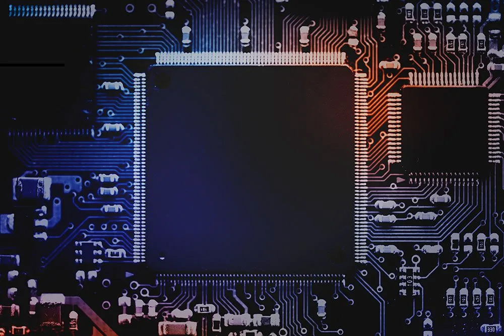
When it comes to the types of ceramic materials, they are classified based on their characteristics, which are combined together in the manufacturing process of ceramic substrates. Usually, metals such as aluminum are used as substrates. Because it has good heat transfer or dissipation performance. Although copper also has heat dissipation properties, its cost is higher compared to aluminum materials.
According to the material, ceramic PCBs can be divided into different types
Aluminum oxide ceramic PCB
Aluminum Nitride PCB
Beryllium oxide PCB
Boron nitride PCB
Silicon carbide PCB
According to the material, ceramic PCBs can be divided into different types of manufacturing processes
Thick film ceramic PCB
Thin film ceramic PCB
Mixed ceramic PCB
Low temperature co fired ceramic (LTCC) PCB
High temperature co fired ceramic (HTCC) PCB
Direct Copper Coated Ceramic (DCB) PCB
Laser activated metalization (LAM) PCB
Thick film ceramic PCB
Thick film ceramic PCB is commonly referred to as thick film resistor ceramic PCB. This technology uses resistor molding to provide embedded resistors on PCBs. Form resistors on the PCB and perform laser trimming on the resistors manufactured on the PCB to ensure that all resistors have the same ohm value or different values. This helps to free up top-level space for active component placement and miniaturization purposes.
Thin film ceramic PCB
This technology is particularly used for manufacturing ceramic core PCBs. It is commonly used in thick film and thin film manufacturing methods. Vacuum deposition: It is difficult to deposit metals on any insulating material, especially on ceramic PCB boards. Due to the use of a special technique called vacuum deposition, the process involves evaporating or sputtering metal on a ceramic substrate. The result of this process is to uniformly add a layer of metal film onto the ceramic substrate.
Mixed ceramic PCB
In this method, different materials are stacked together for specific purposes or applications. For example, 370HR and ceramic aluminum PCB are used in a single stack. The purpose of using 370 HR ceramic is to resist heat. This can improve the performance and efficiency of PCB, thermal management, and so on.
Low temperature co fired ceramic (LTCC) PCB
When manufacturing LTCC, the PCB is placed in a gas furnace at a temperature of up to 900 degrees Celsius. The materials used to manufacture them are powder or crystal glass, metal sheets, and gold paste.
High temperature co fired ceramic (HTCC) PCB
Manufacturing HTCC requires a baking process, which involves baking at a high temperature of 1600 degrees Celsius for more than 40 hours. The materials used to manufacture HTCC include plasticizers, alumina, and mixtures, which are used to mix and bond these materials.
Direct Copper Coated Ceramic (DCB) PCB
During this process, copper and ceramics are bonded together with the help of oxygen. When the material is heated or baked to 1080 degrees Celsius, copper and oxygen combine to form a CuO eutectic liquid, which chemically combines with the ceramic material to form CuAl0O4.
The difference between DPC and DBC: Direct copper plating, as mentioned in the thin film ceramic PCB board method, involves depositing a metal (copper) thin film with a thickness of 10 µ m to 140 µ m on a ceramic substrate through vacuum sputtering process. Direct bonding of copper is a method of bonding copper to ceramic substrates, depositing metal (copper) with a thickness of 140 µ m to 350 µ m.
Laser activated metalization (LAM) PCB
In LAM process, ceramics and metals are ionized through high-power laser drilling technology. The result of this process is the formation of a bond between two substances, resulting in a smoother surface.