Material: Metal based FR4、 High TG FR4 PTFE
The prototype copper is 40 ounces thick
Technology: Backboard, Backdrill, countersunk hole
ISO9001: 2015 certification and UL certification
IPC 600 Level 2 and Level 3
100% electronic testing and AOI inspection
顾名思义,厚铜PCB就是铜比普通PCB厚的PCB。在普通产品中,PCB铜厚约为0.5至2盎司,即17.5至70um。但有些印刷电路板需要比2盎司(70um)更厚的铜厚。因此当铜层上铜箔的成品厚度超过2盎司(70um)时,我们称之为厚铜PCB,也称为极铜PCB。
随着科技的发展,厚铜的应用越来越多,厚铜PCB多用于需要大电流、高可靠性的产品,它存在于我们生活的各个方面,从工业设备到汽车,到白色家电,到电力行业,甚至到军事工业等等,根据铜的厚度不同,产品的应用也有很大的区别。
厚铜板大多采用FR4材质,但也有采用聚酰亚胺材质的,称为厚铜挠性板,此外也有采用铝基、铜基材质的。
Thick copper is chosen by engineers because it has characteristics that cannot be achieved with any smaller copper thickness. Especially with the rapid development of technology, electronic products have increasingly high requirements in various aspects, such as high current and voltage requirements, small size requirements, extremely high reliability requirements, anti-interference, thermal and electrical conductivity requirements, extremely extreme usage environments, etc. Thick copper PCBs can fully meet these strict requirements. Let's take a look at the characteristics of thick copper PCB or extreme copper PCB.
Firstly, it can effectively simplify the volume and withstand larger currents and voltages.
Secondly, its ductility and heat dissipation rate are much stronger than ordinary PCBs.
In addition, thick copper plates are insensitive to both high and low temperatures and have strong corrosion resistance, so the service life of thick copper plates is usually much longer than that of ordinary PCBs.
The common uses of thick copper PCBs include high-tech fields such as mobile phones, microwaves, aerospace, satellite communications, network base stations, hybrid integrated circuits, high-power power circuits, as well as various electronic devices such as home appliances and medical equipment. Here are some applications of thick copper PCB boards:
attribute | capacity |
---|---|
copper thickness | 2oz to 40oz |
storey | Layers 1-12 |
Maximum PCB size | 24 x 48 inches |
material | FR4、 Polyimide, aluminum based, copper based |
technology | Countersunk hole and cavity structure |
Thickness | 0.5-10.0mm |
Outline Method | Use mouse bite, V-shaped cutting, and punching for wiring |
Blind hole/buried hole | contain |
Minimum line width/spacing | 60000 (0.15 millimeters) |
Minimum drilling size | 80000 (0.2 millimeters) |
Surface Treatment | HAL、ENIG、 Sinking silver, sinking tin ENEPIG、OSP |
delivery time | 1-4 weeks |
Everything has its advantages and disadvantages, and thick copper PCBs are no exception. Let's analyze the advantages and disadvantages of thick copper PCBs below.
Undoubtedly, thick copper PCBs perform better in many applications that require high reliability, long lifespan, high current or voltage, high thermal conductivity, or extreme environments because their copper thickness is more robust. There are four main advantages:
Capable of withstanding higher currents and voltages
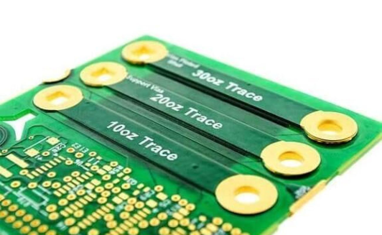
It can be imagined that the thicker the copper on a thick copper PCB, the greater the current it can withstand and the higher the voltage. For example, some high current devices or electric trucks use power PCBs that require huge currents to run, and copper wires with ordinary thickness may burn out, so thick copper in PCBs is necessary. Especially for power modules in trucks or industrial equipment, they may require 10oz or more of copper.
high reliability
The copper thickness used in ordinary PCBs is about 0.5oz to 1oz (or 17.5um to 35um), which is still very thin. PCB thick copper thickness usually exceeds 2oz (70um), with higher current carrying capacity and better heat resistance. In addition, the mechanical strength of copper wires and PTH holes in thick copper PCBs is higher. Therefore, for some products that require very high reliability, such as electronic modules for vehicles and medical requirements, thick copper PCB circuit boards should be used. To avoid copper connection failures in special usage environments.
More heat-resistant, cold resistant, and corrosion-resistant
In addition, thick copper PCB boards are more heat-resistant, cold resistant, and corrosion-resistant than traditional PCBs, so they can be applied to high-end industries above industrial level, military and aerospace level, which can be used in extremely high humidity or hot and cold environments.
Long life cycle
Taking into account these advantages, the service life of heavy copper PCB products is greatly extended, thereby improving the service life of the final product.
Thick copper PCB
Next, let's analyze the drawbacks of thick copper PCBs. Please refer to the following drawbacks of thick copper PCBs:
Cannot be used for high-density PCB routing
For thick copper PCBs, the width and spacing of copper wires should be greater than 6mil, otherwise etching will be more difficult. But in thick copper PCBs, there are also many PCBs with copper wire widths less than 4mil. So thick copper PCBs are not suitable for high-density copper wire PCBs. Does this mean that thick copper PCB circuit boards are typically used for power modules rather than signal modules? Of course it is.
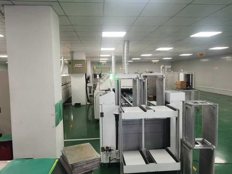
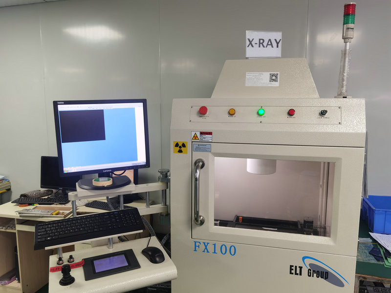
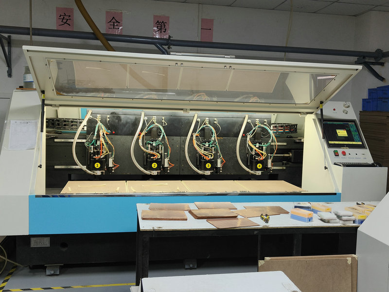
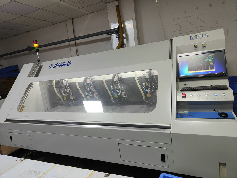
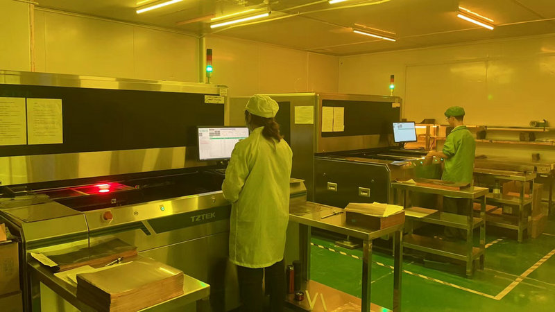
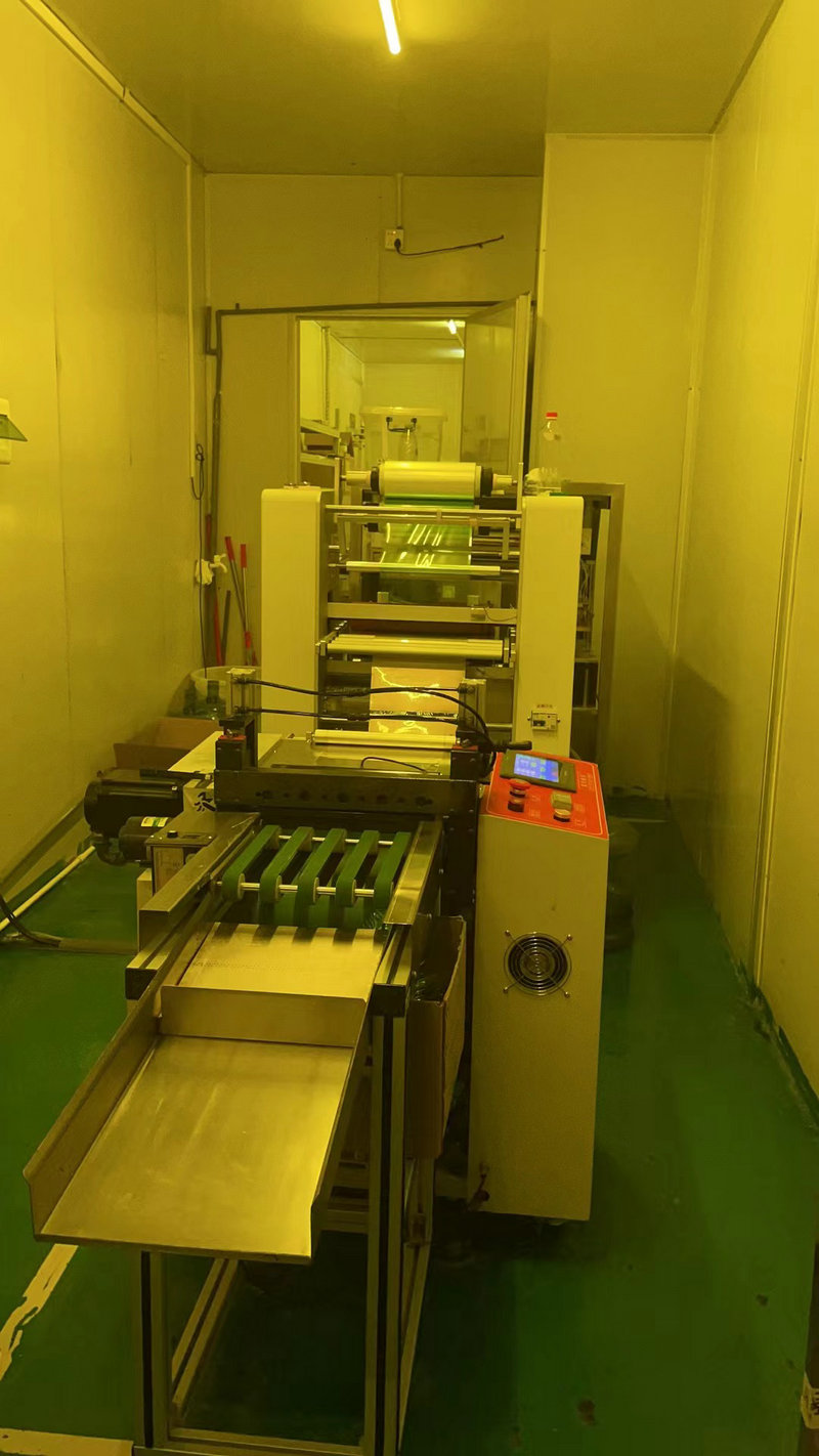
Difficulties in PCB manufacturing
If someone says, 'There are no difficulties in etching and pressing steps for manufacturing thick copper PCBs,' then they are completely wrong. Generally speaking, the thicker the copper thickness, the more difficult it is to etch. Another major difficulty is lamination: due to the large gap between the etched traces, too much resin is required for lamination. If the gap is not properly filled with resin, delamination may occur after PCB assembly, which is an unbearable functional failure. In addition, for thick copper PCBs, solder mask printing is more challenging, but if the lamination is done perfectly, this is not a problem.
High cost
Many people think like this: 'The downside is predictable. Does the more copper used, the higher the cost of heavy copper PCBs? Impossible.' Especially for PCBs with a copper content of 4oz (140um) or more, heavy copper is even more expensive because the more copper is needed, the longer the production time of the substrate. In addition, the amount of heavy copper in PCBs is also more difficult for heavy copper PCB manufacturers to produce, which can lead to an increase in the cost of overweight copper PCBs.
The following are thick copper PCB design specifications for reference.
In addition to design and production, advanced materials also help reduce problems in heavy copper PCB manufacturing. More importantly, these materials help achieve better performance and meet customer requirements. Here are some materials that should be helpful.
RTF copper foil is usually the preferred material for heavy copper PCB manufacturers, mainly to meet the requirements of good heat resistance, corrosion resistance, and the ability to carry large currents and voltages. Why not choose standard copper? Because the Ra value of RTF (Reverse Processed Foils) is smaller than that of standard copper, it is more suitable for withstanding high voltage. In addition, extreme copper PCBs usually use two or more pieces of material, which has many advantages such as a lower probability of breakdown and higher product stability. In addition, if there is a problem with a certain part of the material, it can be repaired, but if there is a problem with the entire material, it cannot be repaired. The characteristic of copper is its good ductility, which can meet various processing requirements.
When the inner copper thickness is greater than 4 ounces, based on past production experience, people usually use PP powder or resin filling to solve the high copper thickness filling solution. However, the disadvantages of this approach are also obvious. Firstly, the thickness is difficult to control, and the process is complex and the cycle is long. Therefore, with the advancement of technology, many thick copper PCB manufacturers, including Weisheng, now use the latest filling materials in the production of PCB thick copper plates. Firstly, the PCB surface is smoother after pressing, and secondly, the resin has better heat resistance and lower expansion coefficient. A high resin content will make the filling effect better, complementing each other. The special structure will also further improve reliability.
Someone may argue, 'If the copper thickness of the substrate with high thermal conductivity is higher, can a PCB with strong heat dissipation be formed to meet the increasing demand in technology?' Yes, it can. The thermal conductivity and heating rate of its finished product will be greatly improved. Compared with ordinary PCBs, the heating rate of thick copper PCBs can be reduced by about 10 °. For PCB, it is a huge progress. There will be more and more research in this area in the future, and most thick copper PCB manufacturers are working hard in this field to seize the opportunity.
In summary, the application of thick copper PCBs will become increasingly widespread in the future. Haibo and other manufacturers of thick copper PCBs will continue to work in this field, seeking better and more powerful production solutions and more advanced materials to produce the highest quality thick copper PCBs for our customers. In addition to thick copper rigid PCBs, we can also provide thick copper flexible PCBs, thick copper rigid flex PCBs, thick copper aluminum PCBs, and copper based PCBs. If you have any requirements for such special projects, please send us your documents for quotation. We look forward to serving you in the future.
If pursuing cost-effective FPC manufacturing services, choosing a Chinese manufacturer is the best choice. As a manufacturing powerhouse, China has abundant resources, cheap labor, and a large number of technical personnel. We recommend Haibo, a Chinese FPC assembly service provider with over 10 years of experience, who has performed outstandingly in various aspects
Efficient and reasonable quotation:There is an efficient quotation process to assist you in making decisions, providing reasonable prices and highly competitive quotes in China.
High quality and reliable products:Produce high standard printed circuit boards, manufacture and test according to specifications, international standards, and internal controls, and conduct pre production inspections to ensure robust processes.
Quick and on-time delivery:The assembly equipment is in good condition, with high productivity, minimal downtime, short delivery time, and also provides urgent services.
Timely and effective response:Always respond to customer needs, provide accurate information, answer questions through multiple channels, and offer one-stop services.
Strong technical strength:China's FPC manufacturing technology is leading, and Haibo has a complete SMT solution that covers assembly, inspection, and other capabilities. It also provides prototype production and customization services.
mobile phone: 86-15113315665
Contact: Chen Changhai
mobile phone: 86-18676922028
E-mall: haibo_fpcba1668@163.com
Address: 3rd Floor, Building 2, Fuxing Industrial Park, Building B, Chuangye 1st Road, Jiangbian Community, Songgang Street, Bao'an District, Shenzhen