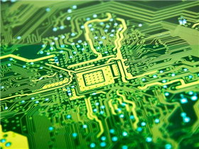
PCB design is usually carried out in stages. Systematically designing PCB boards is much better because it can speed up the process and reduce the likelihood of errors. Printed circuit board (PCB) design can be roughly divided into the following stages:
Requirement and Concept Analysis
Firstly, it is necessary to describe the usage requirements, concepts, and scope of PCB. Clearly describing the requirements and their solutions can accelerate the later PCB design process. The requirements should cover all components related to regulatory, electrical, mechanical, environmental compliance, and cost aspects.
scheme design
Since all requirements have been studied and classified, schematic design can begin. Schematic design is the logical and visual representation of electronic circuits, typically created on EDA tools. The schematic netlist and BOM (Bill of Materials) are generated at this stage of PCB design. This is crucial for providing satisfactory PCB design services.
PCB layout design
After checking for any errors in the schematic design, the PCB design company begins with PCB layout design. PCB layout is the software representation of a PCB or a blueprint used to generate Gerber files. The schematic file is imported into the PCB layout EDA software. Determine all mechanical aspects such as size and deflection, and then design the PCB according to the determined requirements. After the design is completed, the PCB layout file will undergo DRC (Design Rule Check) to check for any violations of constraints and errors.
Signal integrity and power integrity analysis
Many small and simple designs do not follow this step, but it is recommended that high-speed PCBs follow this step as it is crucial for good PCB design services. In this step, the EDA generated feature files (such as Hyperlynx's HYP and ODB files) are input into the SI tool and checked for power and signal integrity, as well as another DRC. If any errors are found in this step, they need to be corrected in the PCB layout file.
Manufacturing and assembly file generation
This is the core part of PCB design services. After passing all DRC and SI PI tests, a Gerber file containing all layer information will be generated for manufacturing. Generate assembly files (such as pick and place files) for machine assembly and manufacturing of PCBs.
Prototype manufacturing and assembly
In most cases, manufacturing is outsourced, so you must provide PCB manufacturers with Gerber files, manufacturing instructions, and pick and place files for manufacturing and assembly. Once the PCB manufacturing is completed, it will be sent for assembly.
Testing and Startup
Then send the completed circuit board for testing and debugging. If any errors are found, the schematic or PCB layout needs to be corrected and the following steps repeated until testing and debugging are unsuccessful.
Design freeze and production
After comprehensive testing of the prototype, the design files will be frozen for future reference, and the PCB will be sent to production. During the production process, the selection will be based on the supplier's production and technical capabilities, as well as the prices offered. At this stage, all economic strategies will be used to reduce the cost of each PCB.
Your trusted partner and one-stop supplier for FPC/PCB manufacturing, component procurement, FPC/PCB assembly, and electronic manufacturing. With over 16 years of experience, we have been providing high-quality FPC/PCB at competitive prices to over 1000 customers worldwide. Our company has passed ISO9001:2015 certification and UL certification, and all of our products have undergone 100% electronic testing and passed AOI and X-RAY inspections to meet the highest industry standards. Therefore, please obtain an immediate quote from our sales team as we will handle the remaining matters.
Haibo is an expert in the field of FPC/PCB manufacturing and surface mount assembly in China. Since our establishment in 2017, we have been providing high-quality PCBs to over 1000 customers worldwide. Our factory has passed ISO14001, ISO9001:2015, TS16949, and ISO13485:2016 certifications. We are one of the most trusted small and medium-sized FPC/PCB manufacturers in China.