Before production, engineers from the PCB manufacturing company will review the Gerber files and recommend suitable materials and stacking to meet the customer's impedance requirements. Please refer to the following impedance matching techniques provided by our engineers for control.
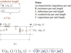
Dielectric thickness and appropriate stacking
Increasing the thickness of the medium can increase the impedance value, while reducing the thickness of the medium can decrease the impedance value. Engineering design, laminated board pressing control, and incoming material tolerance are key factors in controlling the thickness of the medium.
The width/spacing of the conductor meets the impedance value
Increasing line width can reduce impedance, while reducing line width increases impedance. The line width is mainly controlled through etching and design.
The thickness of the conductor meets the impedance value and can also be produced
Reducing the thickness of the conductor can increase the impedance value, while increasing the thickness of the circuit can reduce the impedance. The thickness of the wire can be controlled by graphic electroplating or selecting the corresponding thickness of the base copper foil.
The thickness of the solder mask layer meets the impedance value and can also be produced
Generally speaking, printing a solder mask on a PCB will reduce the impedance value: the single end will decrease by 2 ohms, and the difference will decrease by 8 ohms. Two solder mask layers will reduce the impedance by two times. Printing the solder mask layer three or more times should help reduce the impedance value.
Your trusted partner and one-stop supplier for FPC/PCB manufacturing, component procurement, FPC/PCB assembly, and electronic manufacturing. With over 16 years of experience, we have been providing high-quality FPC/PCB at competitive prices to over 1000 customers worldwide. Our company has passed ISO9001:2015 certification and UL certification, and all of our products have undergone 100% electronic testing and passed AOI and X-RAY inspections to meet the highest industry standards. Therefore, please obtain an immediate quote from our sales team as we will handle the remaining matters.
Haibo is an expert in the field of FPC/PCB manufacturing and surface mount assembly in China. Since our establishment in 2017, we have been providing high-quality PCBs to over 1000 customers worldwide. Our factory has passed ISO14001, ISO9001:2015, TS16949, and ISO13485:2016 certifications. We are one of the most trusted small and medium-sized FPC/PCB manufacturers in China.