1-40 layers, combining rigidity, flexibility, and a combination of rigidity and flexibility
Impedance control, back drill, heavy copper 40 ounces
FR4、 High speed, high frequency, metal core, ceramic PTFE
Blind and buried holes, micropores, arbitrary layer HDI
VIPPO, Blockage of conductive and non-conductive vias
Backboard, embedded devices, IC carrier board
我们都知道 PCB 是印刷电路板的简称。它是我们在每个电子设备中都能看到的绿色、白色或黑色电路板。PCB 是各种电子元件的载体,它通过内部的铜线连接所有这些元件。
所以PCB制造从狭义上讲就是印刷电路板的生产过程。但实际上,制造PCB板涉及到印刷电路板行业的很多知识,包括PCB的历史、PCB的术语、PCB使用的基板、PCB板制造工艺、PCB验收标准、PCB的分类、PCB制造服务的成本、PCB板制造的现状和未来……等等。在这里,海博想和大家分享这些知识,希望对大家有所帮助。
海博是中国的 PCB 制造供应商。我们专注于中小型专业 PCB 制造,拥有 16 年的经验。我们的工厂已通过 UL 认证(E358677)、ISO9001 和 ISO13485 认证。
高TG FR4、无卤素FR4、高速FR4、增强FR4
PI(聚酰亚胺)、PET、半柔性材料
铝、铜、氧化铝陶瓷、特殊合金
RO4350B、RO4003C、RO3003、Arlon 85N、33N、MEGTRON 6(R-5775)、TU-872 LK、Isola Tachyon 100G、ITEQ IT-968TC 等。
层数很重要 | 量产层数为 1-40 层,原型层数可达 100 层 |
板厚 | 0.1-15mm |
最大板尺寸 | 20 * 59英寸 |
最大纵横比 | 16:1 |
阻焊膜颜色 | 绿色、黑色、蓝色、红色、白色(常规颜色),其他颜色按要求提供) |
丝印颜色 | 白色、黑色、黄色(通常),其他颜色按要求) |
大纲方法 | CNC 铣削、V 形切割和冲孔 |
表面光洁度 | HAL、ENIG、浸锡/银、ENEPIG、金手指、镀金、选择性混合 |
In 1925, Charles Ducas of the United States invented printing wires on insulating substrates to replace wire connections, and later adopted electroplated copper wires, marking the beginning of PCB manufacturing.
In 1936, Austrian Paul Eisler invented printed circuit boards and applied them to radio equipment.
In 1947, epoxy resin was used as the substrate in the manufacturing of PCB printed circuit boards.
In 1948, the United States officially recognized the invention of printed circuit boards and used them for commercial purposes.
In 1953, Motorola developed a double-sided board using electroplating through-hole method, which was later applied to the manufacturing of multi-layer printed circuit boards.
In 1960: V. Dahlgren invented flexible printed circuit boards by attaching copper foil to flexible plastic materials. This pioneered the use of flexible materials to manufacture PCBs.
In 1961, Hazeline Corporation in the United States began manufacturing multi-layer PCBs using through-hole electroplating technology. This is a major advancement in PCB manufacturing, as very complex functions can be integrated into multi-layer circuit boards.
In 1995, Panasonic developed arbitrary layer drilling in multi-layer DHI printed circuit boards. Stacked vias are used to meet the connection requirements of any layer.
In 1996, Toshiba developed B2IT multilayer printed circuit boards. Toshiba has developed B2IT multi-layer printed circuit boards. Later, this technology was widely accepted in the PCB board manufacturing industry.
In 2000, new technologies such as rigid flex boards, buried resistors, buried capacitors, and IC carrier boards were being introduced into PCB manufacturing.
We often mention IPC levels 2 and 3 in our daily work, referring to the 600 and 6012 levels in IPC-A-2 and IPC-3, which are also the two most well-known standards in circuit board manufacturing.
IPC-A-600 is a standard for evaluating the acceptability of printed circuit boards according to IPC Level 1, Level 2, or Level 3, used to inspect and distinguish which types of defects are unacceptable to PCB manufacturing suppliers and customers. There are many images that can display the differences between levels 1, 2, and 3. IPC-6012 is a performance specification for PCB manufacturing suppliers, and it is recommended that they work according to IPC Level 1, Level 2, Level 3, or Level 3/A, which focuses more on the production process.
Although IPC-A-600 and IPC-6012 are different files with different uses in PCB manufacturing, their definitions for Level 1, Level 2, or Level 3 are the same. So we don't have to worry about the differences between them.
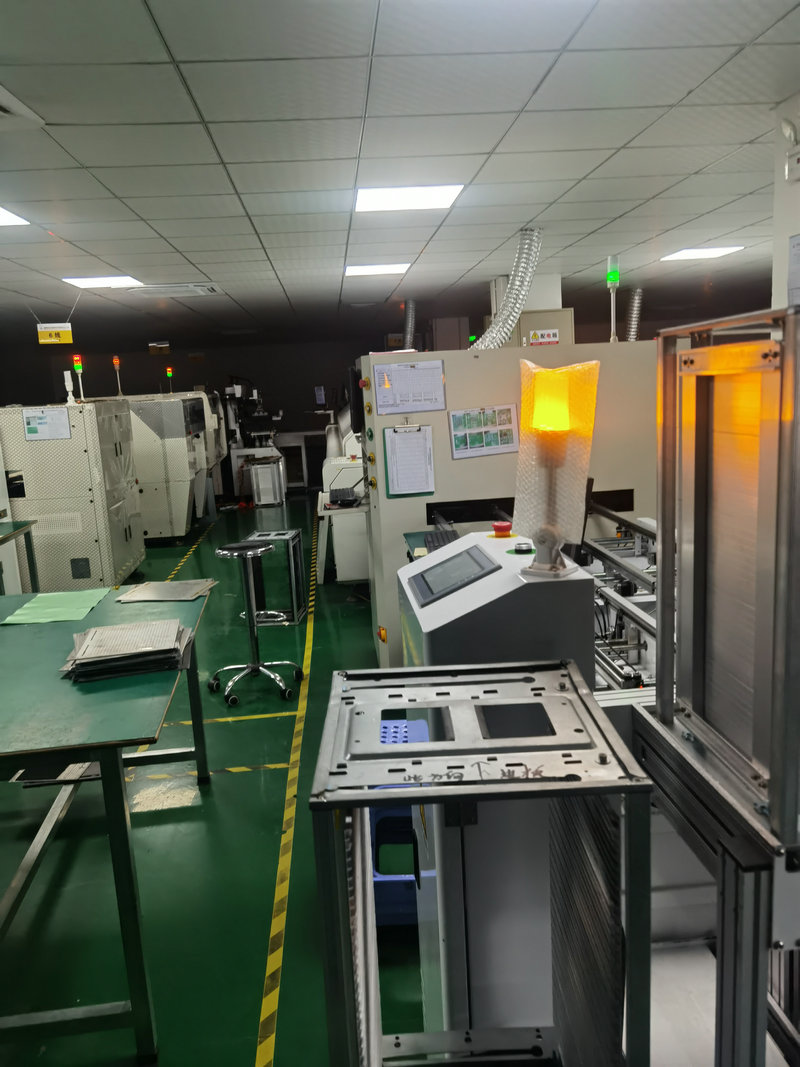
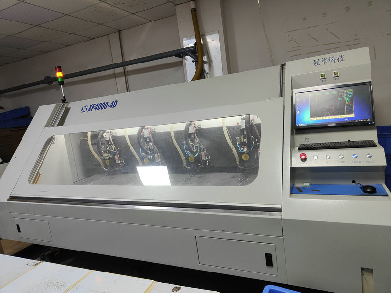
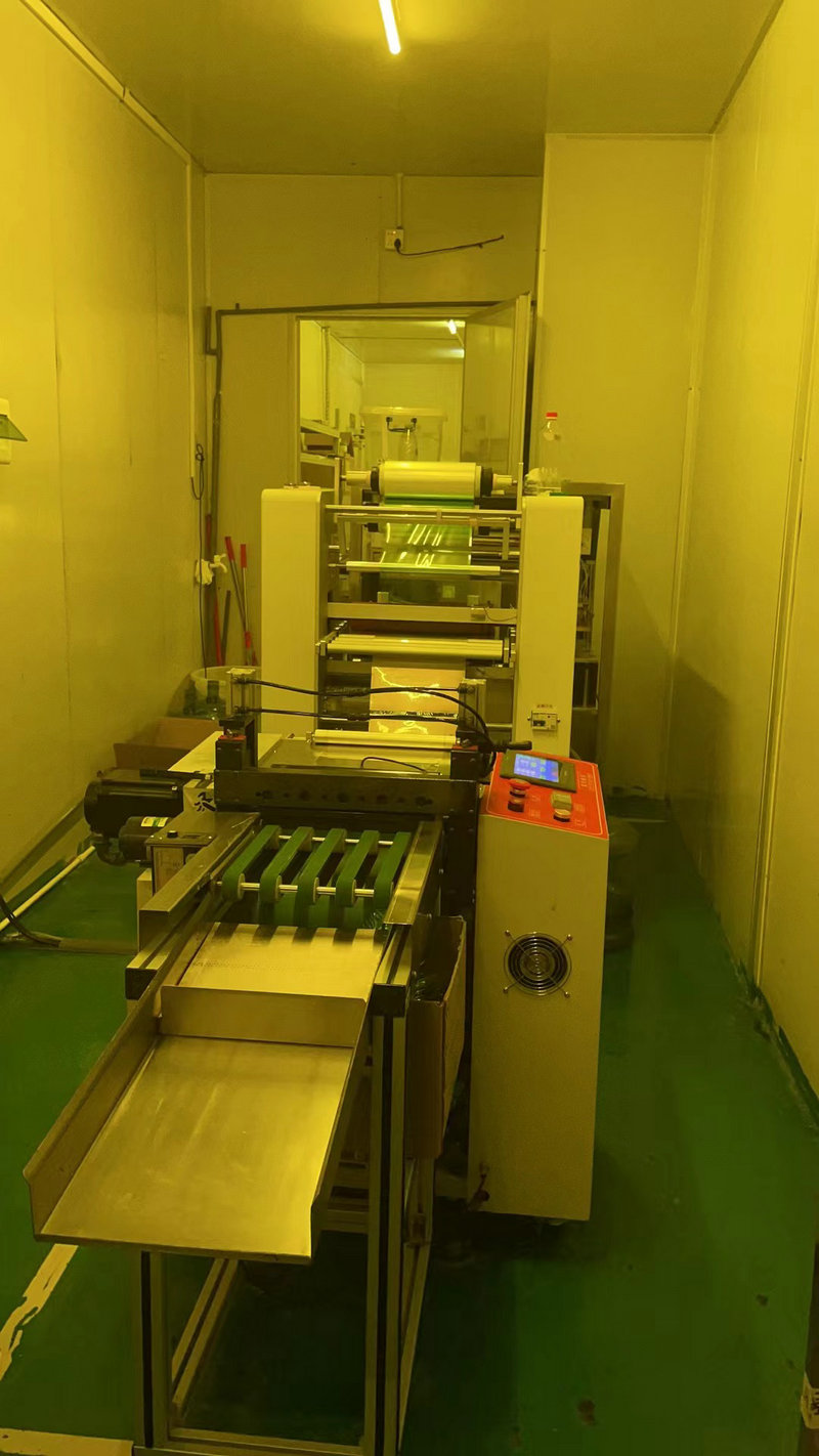
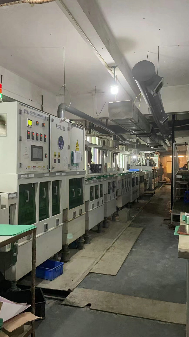
PCB is customized by PCB manufacturing suppliers. Therefore, the cost of each PCB may vary. But we can still provide a quote no matter what. What are the main factors that affect the cost of PCB manufacturing? Please refer to the following detailed information:
This is one of the most important factors, as different types of PCB materials have different price levels, and different companies producing the same type of PCB material may also have significant price differences. Taking the most common PCB material FR4 as an example, its cost may be around $30 per square meter, but the cost of high-frequency materials may be four times higher than that of FR10 materials. Ordinary polyimide materials used for flexible PCBs may cost around $50 per square meter, but polyimide materials from DuPont (the most advanced polyimide material manufacturer) may be 2-5 times higher. Therefore, it is very important to specify the material types in the Gerber files and specifications to PCB manufacturing suppliers.
The larger the PCB crack, the more materials are required to manufacture the PCB, resulting in a higher price. At Viasion, our engineers always strive to provide you with the best advice on PCB panels to achieve optimal utilization in PCB manufacturing services, thereby saving you costs.
The more layers there are, the more materials and production processes are required for circuit board manufacturing, and the higher the cost. Therefore, please use lower layers as much as possible to reduce PCB manufacturing costs.
The thicker the copper, the higher the manufacturing cost of the PCB board. The normal copper thickness is 0.5-1oz, so the price of copper thickness exceeding 1oz will increase. If the copper thickness exceeds 3oz (105um), the PCB manufacturing cost will increase significantly. So it's best to find a PCB manufacturing company for a quotation.
The thicker the overall thickness of the PCB, the higher the cost. The overall thickness of a general PCB is 1.6mm, and the price of PCBs with a thickness exceeding 1.6mm will increase. But the cost of ultra-thin (such as 0.15mm FR4 PCB) rigid PCB is higher than that of general 1.6mm PCB, because the production difficulty of ultra-thin rigid PCB is very high. So in PCB design, it is best to use standard board thickness (0.8 to 2.0mm) to save PCB manufacturing costs.
It is best to use a regular structure for multi-layer PCBs, as special layer structures may incur additional costs in circuit board manufacturing. For example, some engineers have designed very thick dielectrics, which requires stacking several pieces of prepreg together. Extra prepreg means extra cost, and sometimes we even need to add uncovered FR4 material, which will add a lot of cost in PCB manufacturing.
Blind buried holes mean that the PCB manufacturing process is much more complex than ordinary PTH holes and requires more advanced equipment. Therefore, the PCB manufacturing cost of HDI circuit boards is much higher than that of ordinary PCBs with only PTH holes.
The cost of different surface treatment methods also varies. The cheapest ones are HAL and OSP, as well as ENIG. The more expensive ones are silver plating and tin plating ENEPIG, But the most expensive is hard gold plating, with a thickness of about 0.1-3um. It is not difficult to understand that the manufacturing cost of PCB with hard gold plating is very expensive because it is "real gold" plated on the PCB.
Special technologies such as countersunk, back drilling, and impedance may also affect PCB manufacturing costs, so it is best to send Gerber to us for a free quote.
If pursuing cost-effective FPC manufacturing services, choosing a Chinese manufacturer is the best choice. As a manufacturing powerhouse, China has abundant resources, cheap labor, and a large number of technical personnel. We recommend Haibo, a Chinese FPC assembly service provider with over 10 years of experience, who has performed outstandingly in various aspects
Efficient and reasonable quotation:There is an efficient quotation process to assist you in making decisions, providing reasonable prices and highly competitive quotes in China.
High quality and reliable products:Produce high standard printed circuit boards, manufacture and test according to specifications, international standards, and internal controls, and conduct pre production inspections to ensure robust processes.
Quick and on-time delivery:The assembly equipment is in good condition, with high productivity, minimal downtime, short delivery time, and also provides urgent services.
Timely and effective response:Always respond to customer needs, provide accurate information, answer questions through multiple channels, and offer one-stop services.
Strong technical strength:China's FPC manufacturing technology is leading, and Haibo has a complete SMT solution that covers assembly, inspection, and other capabilities. It also provides prototype production and customization services.
mobile phone: 86-15113315665
Contact: Chen Changhai
mobile phone: 86-18676922028
E-mall: haibo_fpcba1668@163.com
Address: 3rd Floor, Building 2, Fuxing Industrial Park, Building B, Chuangye 1st Road, Jiangbian Community, Songgang Street, Bao'an District, Shenzhen