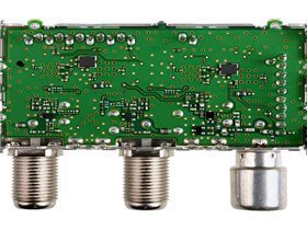
Given the precision required for high-frequency PCB design, we have found that all stages of manufacturing high-frequency PCBs must be carried out with unparalleled caution and precision, as they are naturally used as circuit boards for many devices and applications with sensitive and hazardous tasks, such as medical and military equipment. Therefore, the error rate in the manufacturing process of high-frequency PCB boards must be zero. When starting the manufacturing process of high-frequency PCB boards, please consider the following points.
1. PCB design
The high-frequency PCB manufacturing process begins to ensure the integrity and reliability of the design scheme of the high-frequency PCB board you previously designed. You should conduct all tests on the design to ensure its suitability for manufacturing.
2. Circuit positioning and etching
The design drawings are printed using a dedicated PCB printer. It is printed on the inner copper layer, which is connected to the substrate representing the PCB structure of the board. After completing the printing and engraving process on copper, the inner and outer layers will align perfectly and ensure that they are arranged correctly.
3. Electroplating
Install the inner and outer copper layers separately after plating, and collect the inner and outer layers.
4. Drilling
After the layering process is completed, the drilling process begins, using drilling equipment such as X-ray machines to identify holes and then proceed with drilling.
5. Circuit board cleaning
After the etching process is completed, clean the circuit board and remove excess copper. Afterwards, the circuit board can be coated with chemicals specifically designed for PCB painting, which help to merge and bond the layers together.
6. Solder mask
Ensure again that the circuit board is completely clean before placing the solder mask layer on it. In order to protect the solder mask layer, copper, and all layers of the high-frequency PCB, screen screening and precision machining are required
7. Testing and Inspection
The high-frequency PCB board is now ready for testing to ensure the performance of the circuit board, such as insulation testing, electrical performance of the circuit board, and other tests required to ensure smooth operation of the circuit board.
However, if a company cannot guarantee that all these considerations are met with high capability and efficiency, accurately and reliably executing all these stages, the likelihood of errors occurring during the manufacturing process will be high. Therefore, you must have confidence in who you are dealing with from the beginning to ensure the production of high-quality high-frequency PCB boards.
Your trusted partner and one-stop supplier for FPC/PCB manufacturing, component procurement, FPC/PCB assembly, and electronic manufacturing. With over 16 years of experience, we have been providing high-quality FPC/PCB at competitive prices to over 1000 customers worldwide. Our company has passed ISO9001:2015 certification and UL certification, and all of our products have undergone 100% electronic testing and passed AOI and X-RAY inspections to meet the highest industry standards. Therefore, please obtain an immediate quote from our sales team as we will handle the remaining matters.
Haibo is an expert in the field of FPC/PCB manufacturing and surface mount assembly in China. Since our establishment in 2017, we have been providing high-quality PCBs to over 1000 customers worldwide. Our factory has passed ISO14001, ISO9001:2015, TS16949, and ISO13485:2016 certifications. We are one of the most trusted small and medium-sized FPC/PCB manufacturers in China.