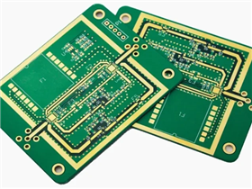
Firstly, the design of a rigid printed circuit board must be generated by drawing circuits in computer-aided design software. The schematic uses pin references for each connection to assign each component to a rigid printed circuit board. Then proceed with PCB layout to display the final physical appearance of the rigid circuit board.
lamination
In the lamination process, the prepreg is laminated with copper foil at high temperature and high pressure. The prepreg is composed of uncured resin, and during the lamination process, high temperatures can cause the resin to become viscous and eventually cure. This process is carried out in a closed hot press machine.
Application of photoresist
The application of photoresist is an essential step in the manufacturing of rigid PCBs, in order to form a protective layer on the easily oxidizable copper layer. During this process, positive photoresist is a widely used technique, in which the portion of photoresist exposed to ultraviolet light becomes highly soluble in developer chemicals. Some commonly used developer solutions are sodium hydroxide or alkaline solutions.
Etching process
The next step in producing rigid PCBs is to etch away unwanted copper patterns using etchants such as ferric chloride and ammonium chloride. In order to obtain consistent and high-quality copper patterns, it is necessary to specify and control the etching rate and etching solution concentration. Etching can be carried out through immersion, spray etching, or sputtering methods. After the etching process, there is a rinsing step to clean the remaining photoresist.
drilling
Use a computer programmable drilling machine to drill and conduct holes. Small electronic components require drill bits with smaller diameters. For fiberglass rigid PCBs, diamond tungsten carbide drill bits are being used. Accurate drilling must be achieved by optimizing drilling speed, force, and geometry. Usually, boards are stacked together to drill holes simultaneously. There are various types of drilling techniques, such as laser, micro drilling, and micro machining.
Solder mask
Solder mask, also known as "solder mask", is applied to rigid printed circuit boards. Welding masks are used as protective coatings to isolate conductive and insulating surfaces on rigid PCBs. The photolithography process can be performed using liquid photosensitive imageable solder mask (LPSM) by exposing the photosensitive solder resist to ultraviolet light for curing. Epoxy liquid can also be directly screen printed onto rigid printed circuit boards and thermally cured.
Surface Treatment
The exposed copper part undergoes surface treatment process. Please remember that copper is easily oxidized when exposed to the environment. Although copper is susceptible to corrosion, it remains the preferred basic conductive material due to its excellent thermal and electrical conductivity. Due to the possibility of oxidation during subsequent heat treatment during assembly, surface treatment is required on the exposed solder pads.
Surface treatment ensures effective welding of components. Some surface treatment options include hot air solder leveling (HASL) and electroless nickel immersion gold (ENIG). HASL coats copper with a layer of solder, while ENIG involves nickel and gold plating to ensure good connectivity.
Screen printing
In order to print information on rigid PCBs, screen printing technology is required. PCB information, such as component codes, pin locators, company logos, reference points, regulatory marks, and other traceability labels, can be screen printed on rigid PCBs. There are multiple methods to apply screen printing information to rigid PCBs. One method is to use templates and scrapers to transfer ink patterns onto rigid PCBs. Another method is liquid light imaging (LPI), which is more suitable for high-density rigid printed circuit boards. This method uses photosensitive ink, which is then developed and cured to produce screen printing.
Your trusted partner and one-stop supplier for FPC/PCB manufacturing, component procurement, FPC/PCB assembly, and electronic manufacturing. With over 16 years of experience, we have been providing high-quality FPC/PCB at competitive prices to over 1000 customers worldwide. Our company has passed ISO9001:2015 certification and UL certification, and all of our products have undergone 100% electronic testing and passed AOI and X-RAY inspections to meet the highest industry standards. Therefore, please obtain an immediate quote from our sales team as we will handle the remaining matters.
Haibo is an expert in the field of FPC/PCB manufacturing and surface mount assembly in China. Since our establishment in 2017, we have been providing high-quality PCBs to over 1000 customers worldwide. Our factory has passed ISO14001, ISO9001:2015, TS16949, and ISO13485:2016 certifications. We are one of the most trusted small and medium-sized FPC/PCB manufacturers in China.