PCB公差是指生产出来的PCB与实际的PCB之间在尺寸、厚度、角度、数值等参数上的偏差。 印刷电路板制造商 以及客户的图纸。例如,一块PCB设计为1.6mm厚度,但PCB制造商无法确保所有PCB的厚度都恰好是1.6mm;个别PCB可能比1.6mm厚或薄。那么,就应该有一个公差。对于1.6mm的PCB,公差通常应为±0.16mm,在特殊要求下,公差应低至±0.1mm或更小。
一般来说,公差越严格,制造难度就越大,成品率就越低。但与此同时,公差越严格,功能可靠性就越高。PCB 公差要求也会根据应用和环境而变化。例如,如果 PCB 用于航空航天,则其 PCB 公差可能比用于消费产品的 PCB 公差严格得多。因此,在设计 PCB 时还必须考虑 PCB 公差,因为任何差异都可能导致 PCB 功能不佳。
除了客户图纸的要求外,PCB还有众所周知的行业标准。最常用的是IPC-A-600。PCB制造商应遵守IPC-A-600标准中关于PCB公差要求和验收标准的规定。通过严格遵守PCB公差要求,PCB制造商可以确保PCB的质量和性能。
在海博,我们严格遵循客户的要求和 IPC-A-600 2 级和 3/3A 级公差标准,为客户提供最高质量的 PCB。请参考以下最常用的印刷电路板生产公差。
如果您有任何问题或疑问,请随时与我们联系。
商品描述 | 公差 | 附注 |
---|---|---|
材料厚度 | ≤1.0毫米:±0.1毫米 | |
>1.0毫米:±10% | 最佳:≤2.0mm±0.1mm;2.1-3.0mm±0.15mm;3.1-7.0mm+/-0.25m | |
柔性 PCB 厚度 | +/- 0.025mm | 加强筋面积:+/-0.05mm |
最大弯曲和扭曲 | 0.75% |
商品描述 | 公差 | 附注 |
---|---|---|
镀孔尺寸 (PTH) | ≤4.00毫米+/-0.75毫米 | 最佳:+/- 0.05mm |
>4.00 毫米 +/- 0.10 毫米 | ||
非镀层孔尺寸 (NPTH) | ≤4.00毫米+/-0.05毫米 | |
>4.00 毫米 +/- 0.10 毫米 | ||
钻孔镀槽尺寸(PTH 槽) | +/- 0.1mm | 最佳:+/- 0.75mm |
非镀层槽尺寸(钻孔法)(NPTH 槽) | +/- 0.075mm | 最佳:+/- 0.05mm |
孔位 | +/- 0.075mm | |
背钻深度 | +/- 0.1mm | |
埋头孔角度 | +/- 10° | |
埋头孔尺寸 尺寸 | +/- 0.15mm | |
长宽比 | 1:18 | 钻孔尺寸:PCB厚度 |
商品描述 | 公差 | 附注 |
---|---|---|
最小铜厚度 | IPC A-20 600 级为 2μm | IPC A-25 600 级为 3μm |
商品描述 | 公差 | 附注 |
---|---|---|
无铅喷锡膏 | 2 – 40微米 | |
沉金 (ENIG) | 镍:3-8μm;金:0.05 – 0.10μm | |
沉银 | 0.2 – 0.4微米 | |
浸锡 | >=1.0um | |
OSP | 0.1-0.3um | |
镍钯金 | Ni:3-8um Pa:0.05-0.15um Au:0.05-0.1um | |
电镀金 | 镍:3~6μm;金:0.1~4μm | |
碳墨水 | 0.10-0.35mm | |
可剥面膜 | 0.20-0.80mm |
商品描述 | 公差 | 附注 |
---|---|---|
最小阻焊层与走线间隙 | 0.05mm | |
最小阻焊轨道覆盖 | 0.05mm | |
最小阻焊网 | 0.075mm | |
铜线厚度 | 10-18um | |
铜线边缘厚度 | >10μm |
商品描述 | 公差 | 附注 |
---|---|---|
最小宽度 | 0.10mm | |
最小高度 | 1.00mm |
商品描述 | 公差 | 附注 |
---|---|---|
最小走线/焊盘到轮廓 – 外层 | 0.15mm | |
最小走线/焊盘到轮廓 – 外层 | 0.20mm | |
型材尺寸公差 | +/- 0.13mm | 最佳:+/- 0.13mm |
商品描述 | 公差 | 附注 |
---|---|---|
最大 PCB 厚度 | 3.20 mm | |
最小 PCB 厚度 | 0.60mm | |
最小V-cut铜距离 | 0.3mm | |
分离后的差异 | +/- 0.20mm | |
正常休息材料 | 0.50 毫米 +/- 0.10 毫米 | |
V 形切割位置公差从上至下 | +/- 0.1mm | |
最小分数深度 | 0.1mm |
商品描述 | 公差 | 附注 |
---|---|---|
斜角公差 | +/- 5° | 15°,30°,45°,60° |
剩余材料厚度公差 | +/- 0.1mm |
商品描述 | 公差 | 附注 |
---|---|---|
阻抗容差 | + / - 10% | + / - 5% |
商品描述 | 公差 | 附注 |
---|---|---|
最小测试间距 | 0.10mm | |
最小可测试焊盘 | 0.05mm | |
测试电压 | 500V | |
测试电流 | 200毫安 | 可调整 |
连续性测试 | 最小5Ω | |
隔离测试 | 最大500MΩ |
If pursuing cost-effective FPC manufacturing services, choosing a Chinese manufacturer is the best choice. As a manufacturing powerhouse, China has abundant resources, cheap labor, and a large number of technical personnel. We recommend Haibo, a Chinese FPC assembly service provider with over 10 years of experience, who has performed outstandingly in various aspects
Efficient and reasonable quotation:There is an efficient quotation process to assist you in making decisions, providing reasonable prices and highly competitive quotes in China.
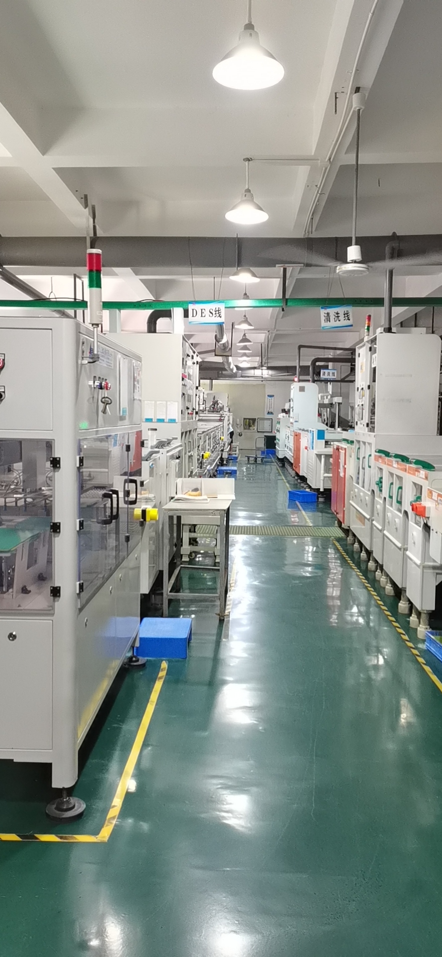
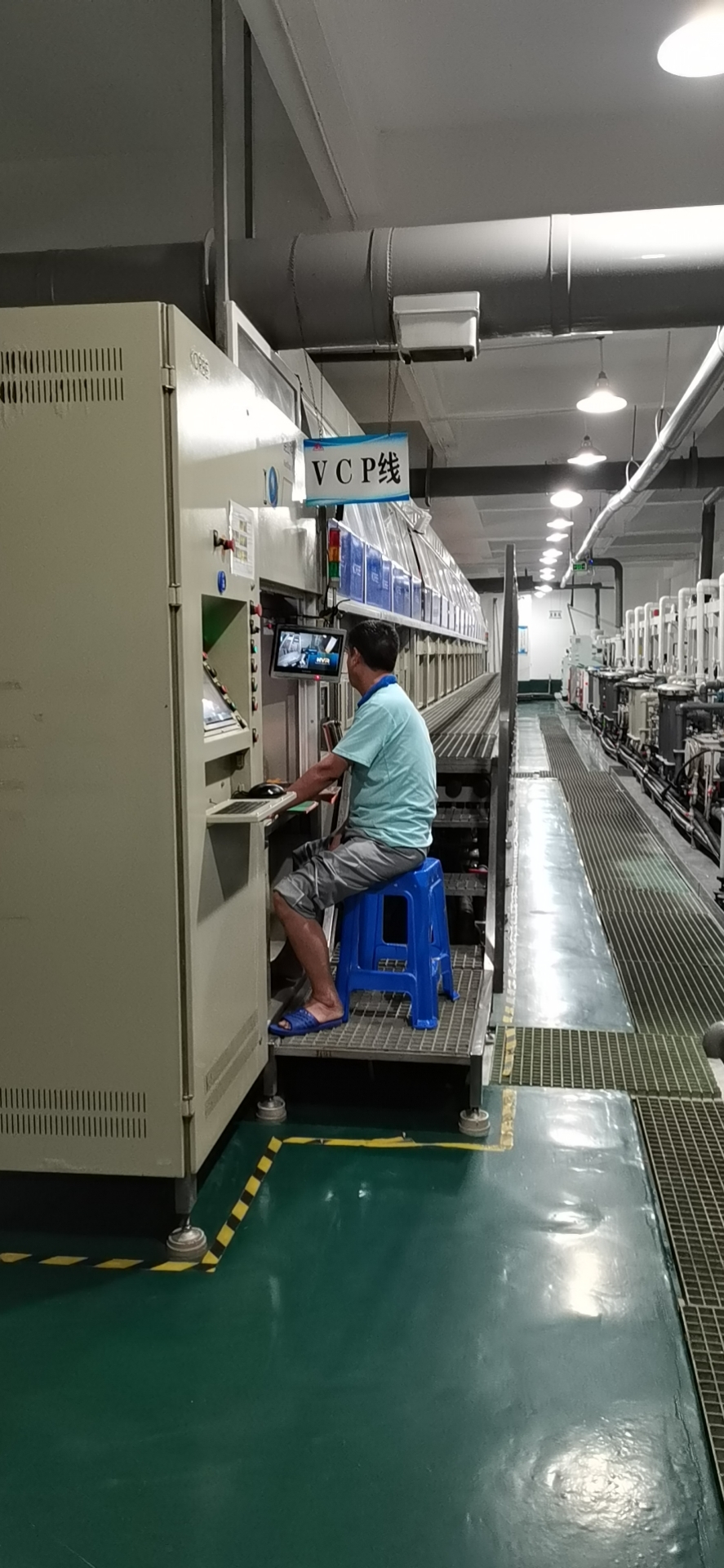
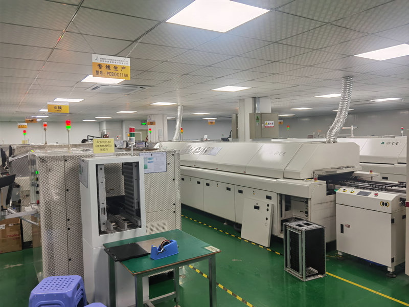
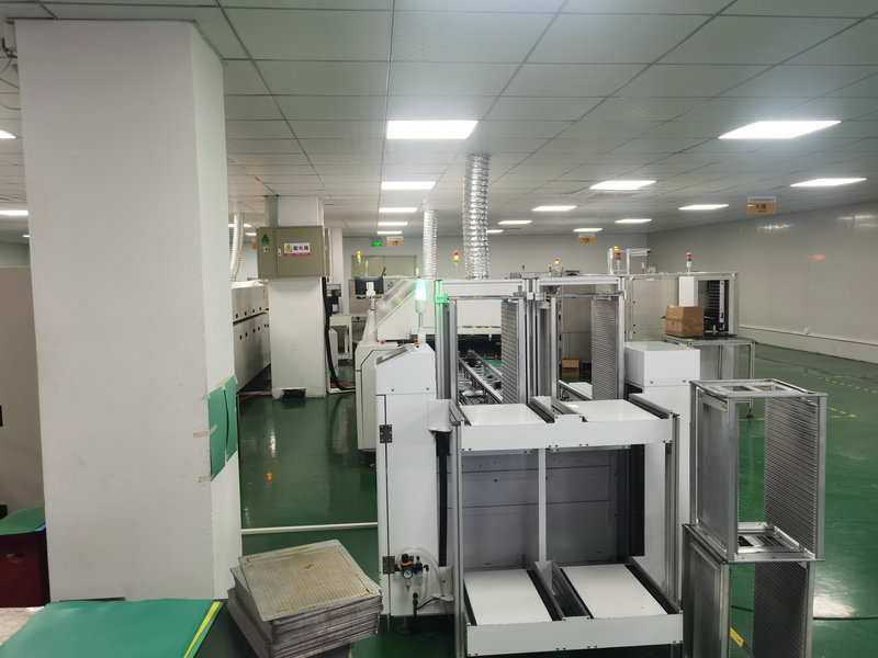
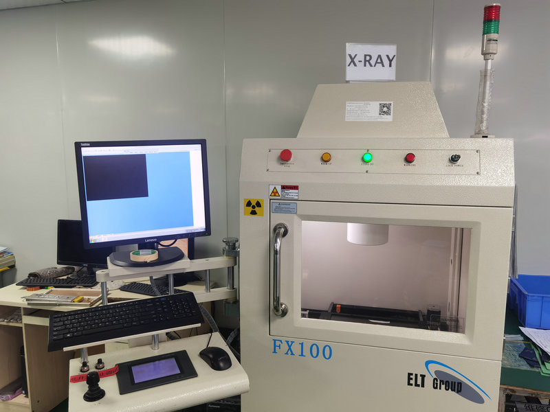
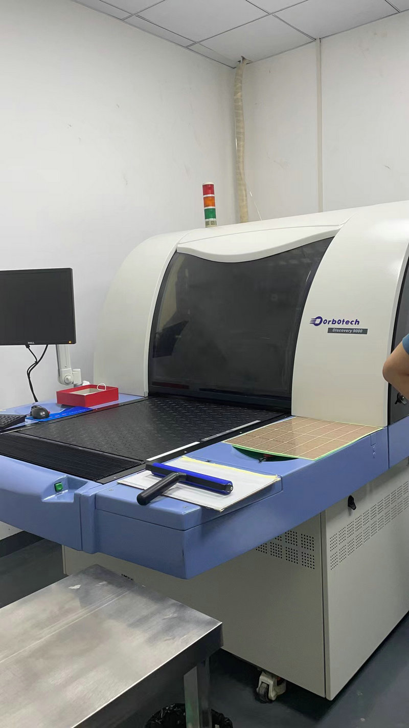
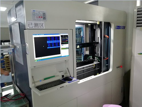
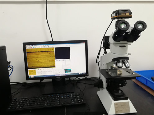
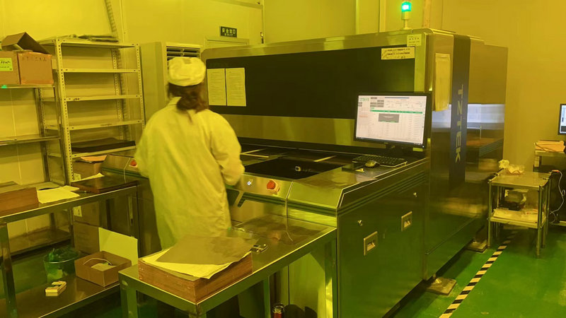
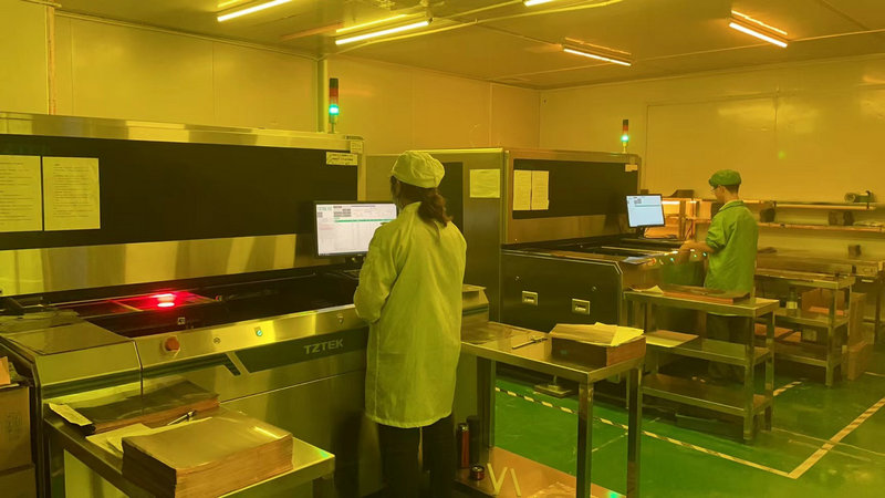
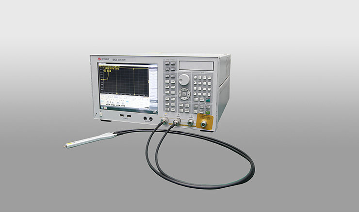
High quality and reliable products:Produce high standard printed circuit boards, manufacture and test according to specifications, international standards, and internal controls, and conduct pre production inspections to ensure robust processes.
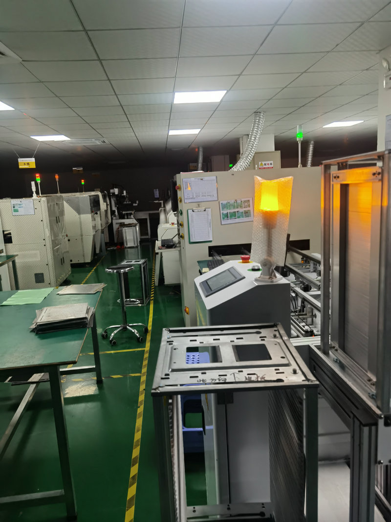
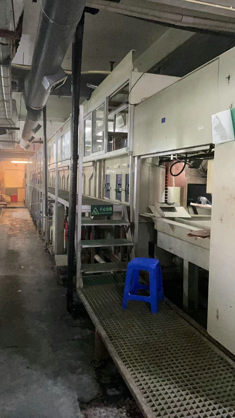
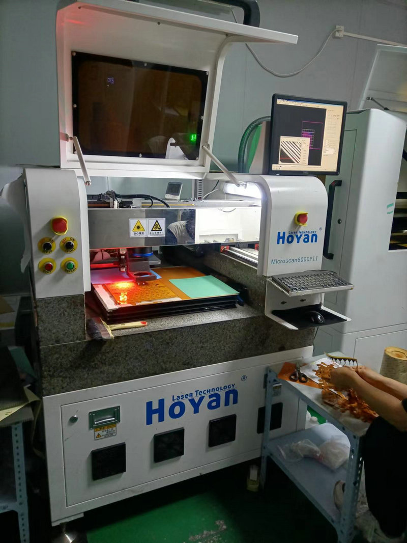
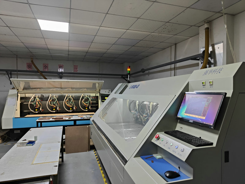
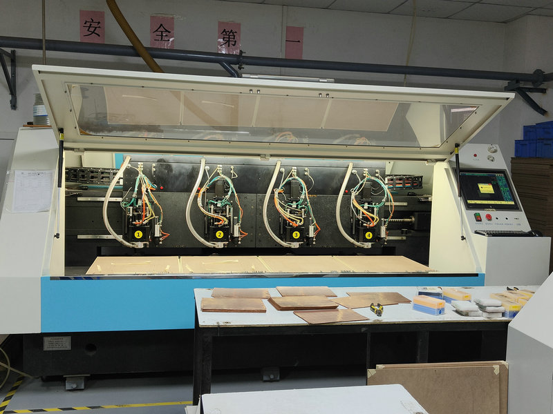
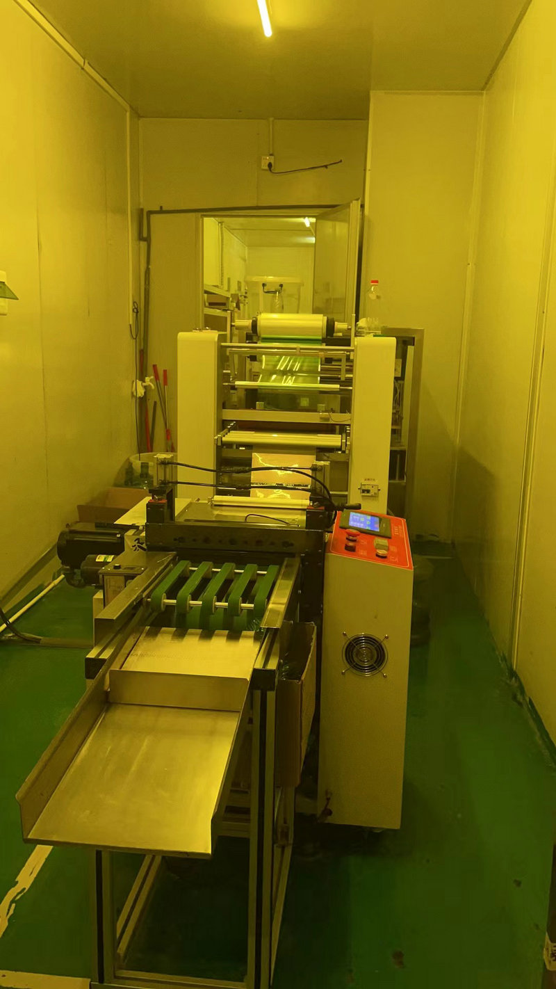
Quick and on-time delivery:The assembly equipment is in good condition, with high productivity, minimal downtime, short delivery time, and also provides urgent services.
Timely and effective response:Always respond to customer needs, provide accurate information, answer questions through multiple channels, and offer one-stop services.
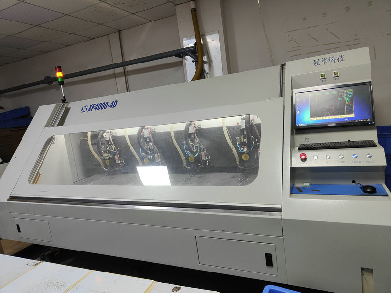
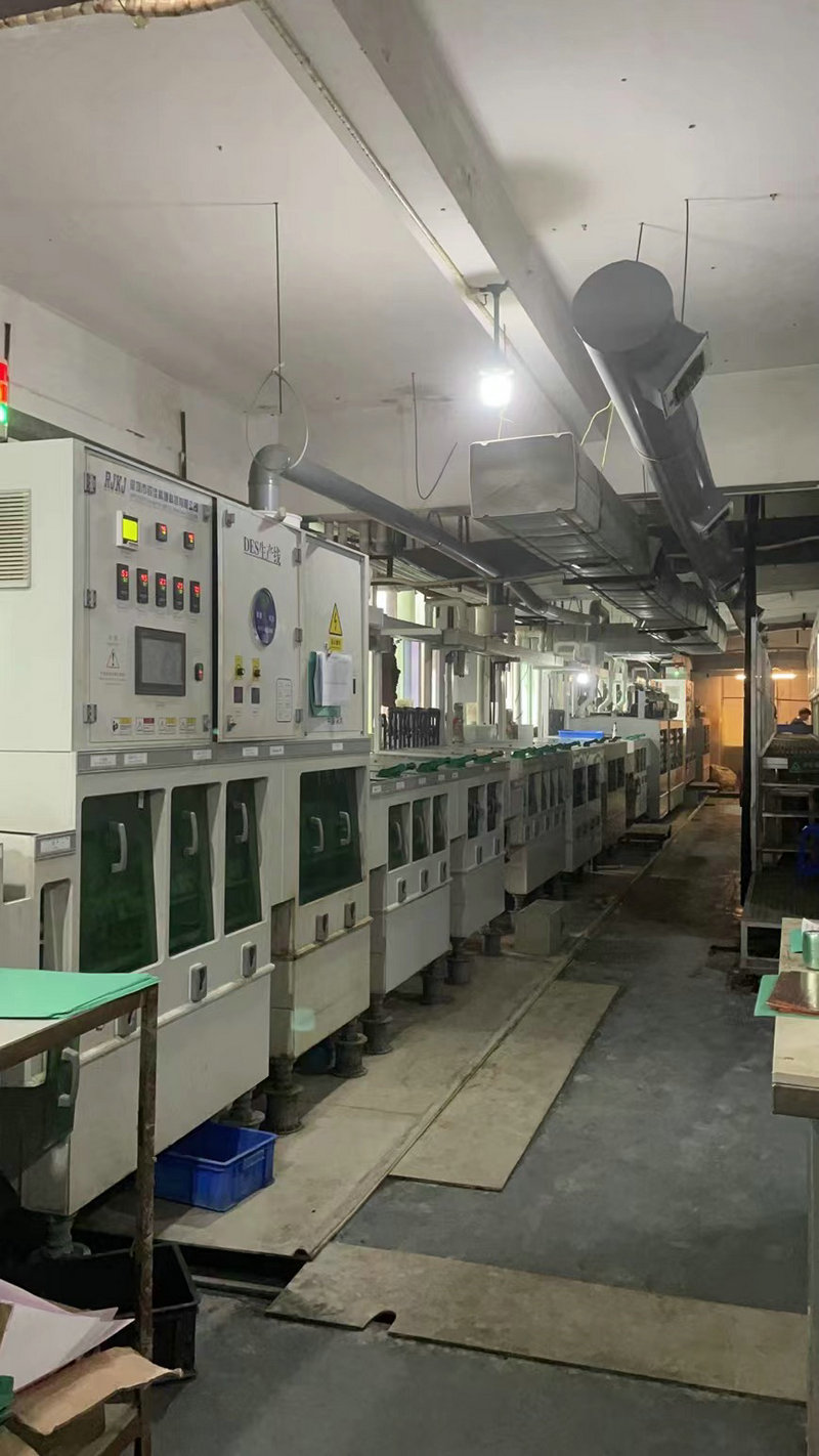
Strong technical strength:China's FPC manufacturing technology is leading, and Haibo has a complete SMT solution that covers assembly, inspection, and other capabilities. It also provides prototype production and customization services.
mobile phone: 86-15113315665
Contact: Chen Changhai
mobile phone: 86-18676922028
E-mall: haibo_fpcba1668@163.com
Address: 3rd Floor, Building 2, Fuxing Industrial Park, Building B, Chuangye 1st Road, Jiangbian Community, Songgang Street, Bao'an District, Shenzhen