PCB Design and Layout
Introduction to Electronic Design and New Products
Component procurement and turnkey PCB assembly
Prototype and small to medium batch production
ISO9001: 2015, Quality Certification
No minimum order quantity and competitive pricing
PCB 几乎无处不在。从手表到飞机,几乎您看到的每台机器都使用 PCB。设计这些 PCB 本身就是一门艺术和科学。PCB 设计需要机械、电子、经济和美学方面的全部知识。以前,由于资源有限且缺乏 CAD 设计工具,即使对于简单的设计,PCB 设计也曾经是一项非常具有挑战性的任务。如今,现代 CAD 和 EDA 工具不仅使定制 PCB 设计中国变得更简单,而且还突破了 PCB 的功能极限。现代 PCB 以更高的速度处理数据,可以在恶劣的环境中运行,能够在更小的区域容纳更小的组件,更重要的是,可以批量生产各种形状和尺寸。什么是 PCB 设计?让我们继续寻找答案。
PCB design is the process of designing a printed circuit board with conductive layers around non-conductive materials and components laid on top of them. Sounds simple, right? However, the process we are discussing is far from simple, as it involves subtle integration of electronics, machinery, software, manufacturing, testing, and economics. It requires perfect compromises in every field to build a perfect printed circuit board (PCB) design. The capabilities of manufacturers and continuous technological advancements have made complex designs very common. Smartphones, wireless headphones, laptops, televisions, etc. are the main examples of common and complex devices designed by PCB design companies.
It is important to understand that the design of a printed circuit board (PCB) will affect the performance of its components and software. A well-designed PCB is the key to fully utilizing the potential of the circuits designed on it.
As mentioned earlier, PCB design is a process that involves multiple factors working together. Now that we know what PCB design is, we must further understand the factors that affect PCB design. Some of them are:
The most important factor affecting the quality of printed circuit board (PCB) design is its electrical performance. The electrical performance is determined by the following factors:
Signal integrity: Signal integrity is a standard for measuring the quality of the signal transmission path on the PCB. High signal integrity ensures that signals on the PCB do not lose power or introduce any noise on the PCB.
Power allocation: Power allocation ensures that all components have sufficient power to operate effectively. Poor power distribution can cause component failures and PCB board overheating.
Material selection: Using appropriate dielectric materials and a suitable amount of copper can affect the electrical performance of the PCB.
Due to poor electrical design, it can cause signal noise, PCB heating during normal operation, voltage fluctuations, etc.
Mechanical considerations are one of the key factors in the design of printed circuit boards (PCBs). The factors that affect the mechanical performance of PCB include:
Specifications: The size of PCB refers to its length and width. Longer PCBs are prone to bending, resulting in mechanical stress on the edges.
Thickness: The thickness of PCB is an important factor in mechanical integrity. Thin PCBs are prone to breakage and bending. Thick PCBs not only increase the weight of the PCB, but also reduce its mechanical integrity.
Flexibility: The flexibility of PCB depends on the material and thickness of the PCB. Polyimide and other materials are flexible to a certain extent, so they are used for PCBs that require bending. It must be noted that rigid PCBs must not be bent before design requirements.
Other mechanical properties include core wire materials, dielectric materials, through-hole types, surface smoothness, etc.
A very important part of custom PCB design is to maintain the economy of the PCB. The economy of PCB is determined by the following factors:
Materials and characteristics used: The materials and characteristics used to manufacture PCBs directly affect the cost of PCBs. The general trend is that the more advanced the features or materials used on the PCB, the more expensive the PCB will be.
The complexity of design: The cost of irregularly shaped and stacked PCBs is usually higher than that of simple shapes such as rectangles and circles.
The supply chain of PCB design companies: The supply chain of PCB design companies is usually the final stage of printed circuit board PCB design and the main factor in PCB cost. Factors such as delivery time, quantity scale, and supplier's geographical location are all included in the supply chain.
The above factors are only a small part of the many factors. If the economic situation is good, even advanced PCBs will become much cheaper.
The requirements for printed circuit board (PCB) design are not as many as before, as most tools are only software used for design and simulation. The requirements for good PCB design services are:
Printed circuit board (PCB) design software or EDA (Electronic Design Automation) tools are necessary for schematic design, PCB layout, 3D visualization tools (3D visualization tools are not necessary, but it is preferable to have them), and Gerber file generation. Usually, most EDA tools provide all of these functionalities in one software. Some examples are OrCAD, Altium, and KiCAD.
SPICE (Integrated Circuit Key Simulation Program) and SI (Signal Integrity) tools are used to simulate circuit behavior, electrical characteristics, and performance parameters. For simpler designs, they are not necessary, but it is recommended to use them. Some examples of SPICE tools are LTSPICE and PSPICE. Some examples of SI tools are AnSys and Hyperlynx.
A very important part of PCB design is circuit board debugging and testing. It requires segmented testing of the circuit board.
PCB design is usually carried out in stages. Systematically designing PCB boards is much better because it can speed up the process and reduce the likelihood of errors. Printed circuit board (PCB) design can be roughly divided into the following stages:
Firstly, it is necessary to describe the usage requirements, concepts, and scope of PCB. Clearly describing the requirements and their solutions can accelerate the later PCB design process. The requirements should cover all components related to regulatory, electrical, mechanical, environmental compliance, and cost aspects.
Since all requirements have been studied and classified, schematic design can begin. Schematic design is the logical and visual representation of electronic circuits, typically created on EDA tools. The schematic netlist and BOM (Bill of Materials) are generated at this stage of PCB design. This is crucial for providing satisfactory PCB design services.
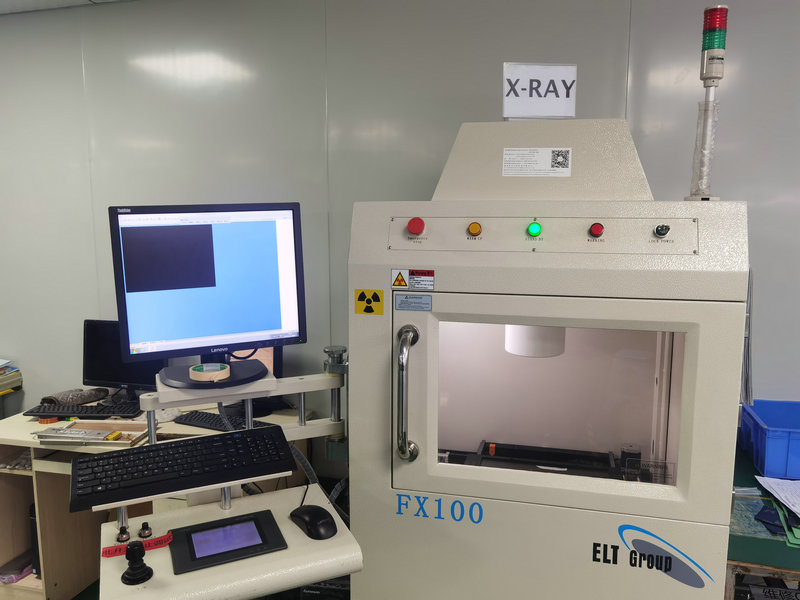
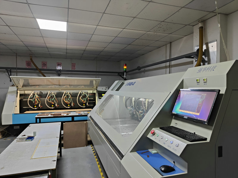
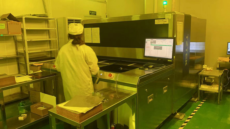
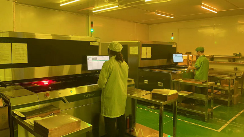
After checking for any errors in the schematic design, the PCB design company begins with PCB layout design. PCB layout is the software representation of a PCB or a blueprint used to generate Gerber files. The schematic file is imported into the PCB layout EDA software. Determine all mechanical aspects such as size and deflection, and then design the PCB according to the determined requirements. After the design is completed, the PCB layout file will undergo DRC (Design Rule Check) to check for any violations of constraints and errors.
Many small and simple designs do not follow this step, but it is recommended that high-speed PCBs follow this step as it is crucial for good PCB design services. In this step, the EDA generated feature files (such as Hyperlynx's HYP and ODB files) are input into the SI tool and checked for power and signal integrity, as well as another DRC. If any errors are found in this step, they need to be corrected in the PCB layout file.
This is the core part of PCB design services. After passing all DRC and SI PI tests, a Gerber file containing all layer information will be generated for manufacturing. Generate assembly files (such as pick and place files) for machine assembly and manufacturing of PCBs.
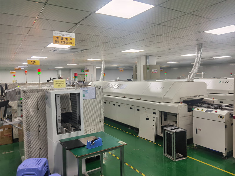
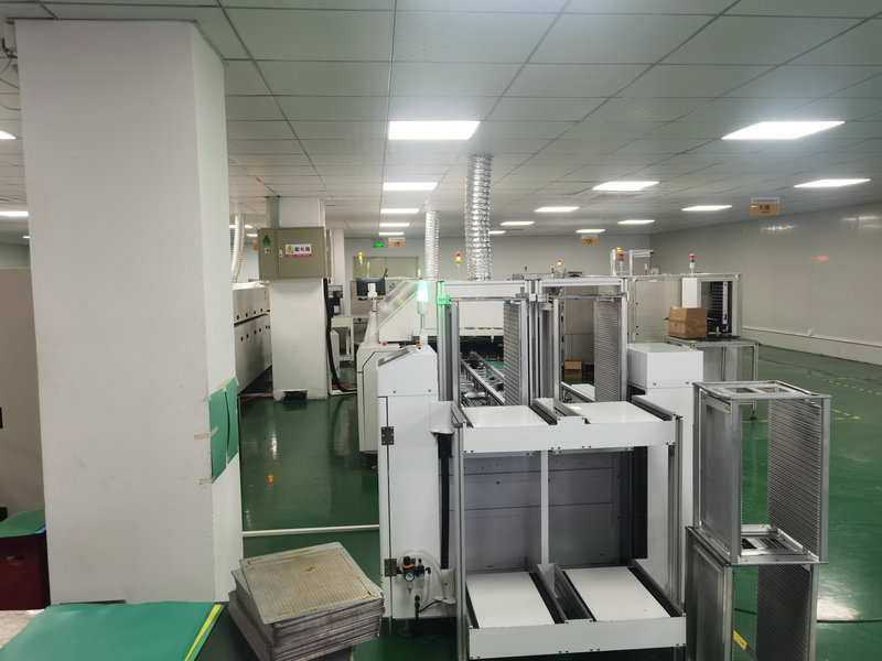
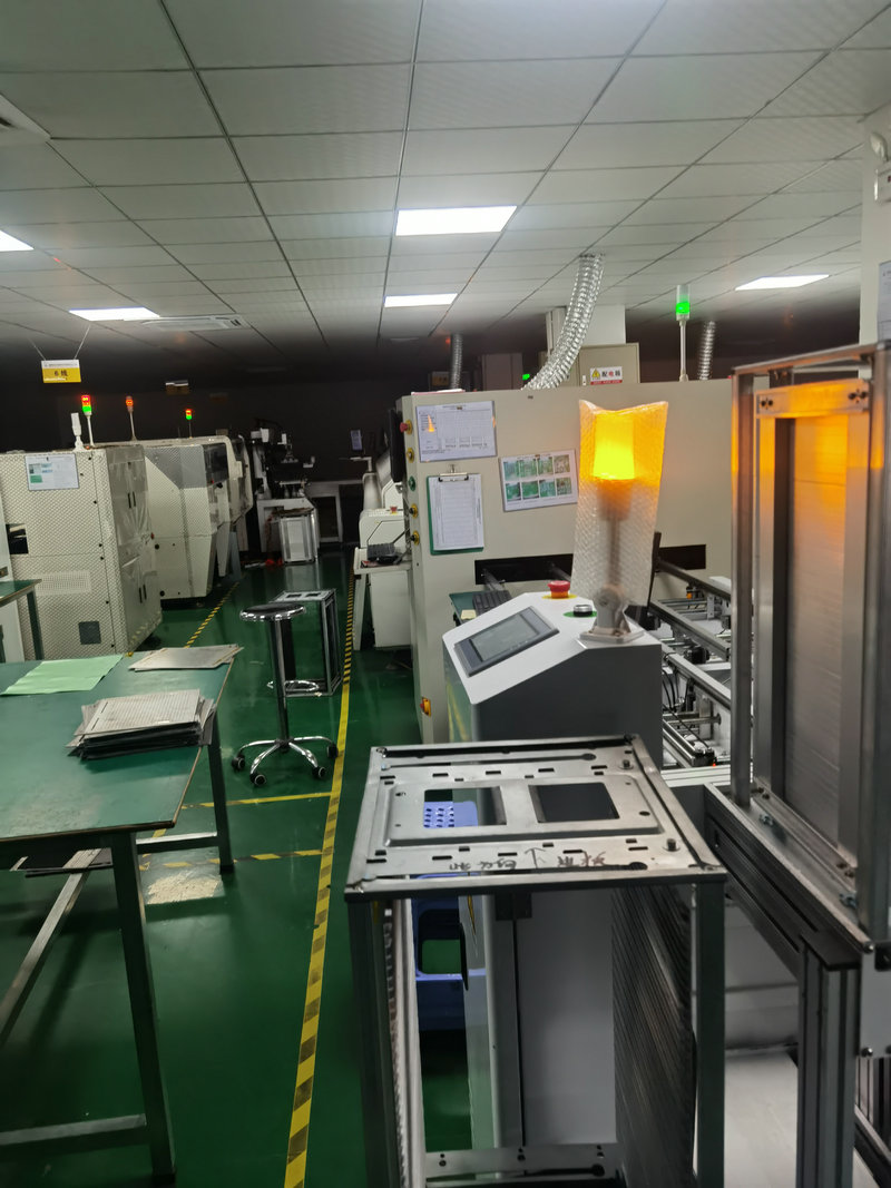
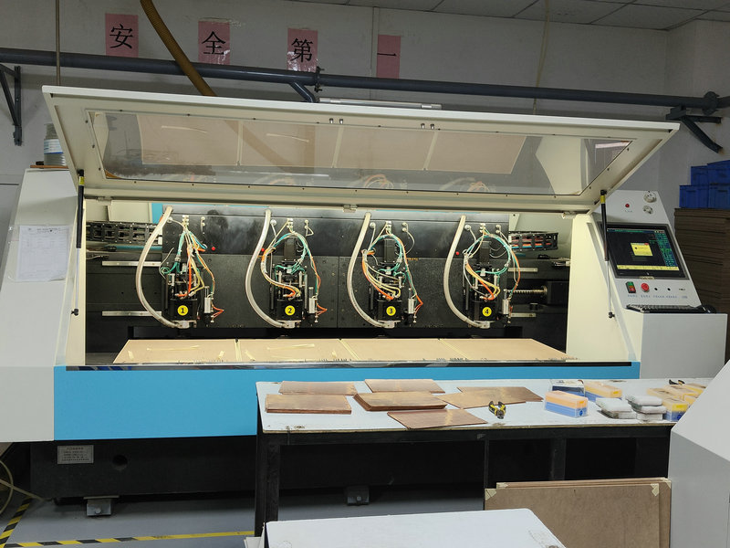
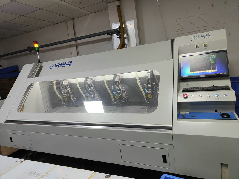
In most cases, manufacturing is outsourced, so you must provide PCB manufacturers with Gerber files, manufacturing instructions, and pick and place files for manufacturing and assembly. Once the PCB manufacturing is completed, it will be sent for assembly.
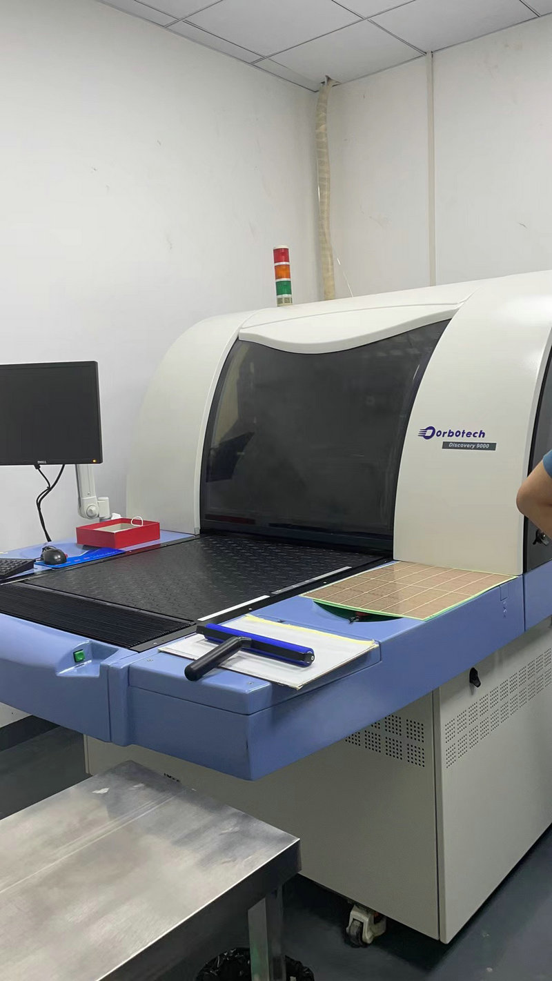
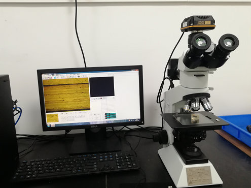
Then send the completed circuit board for testing and debugging. If any errors are found, the schematic or PCB layout needs to be corrected and the following steps repeated until testing and debugging are unsuccessful.
After comprehensive testing of the prototype, the design files will be frozen for future reference, and the PCB will be sent to production. During the production process, the selection will be based on the supplier's production and technical capabilities, as well as the prices offered. At this stage, all economic strategies will be used to reduce the cost of each PCB.
If pursuing cost-effective FPC manufacturing services, choosing a Chinese manufacturer is the best choice. As a manufacturing powerhouse, China has abundant resources, cheap labor, and a large number of technical personnel. We recommend Haibo, a Chinese FPC assembly service provider with over 10 years of experience, who has performed outstandingly in various aspects
Efficient and reasonable quotation:There is an efficient quotation process to assist you in making decisions, providing reasonable prices and highly competitive quotes in China.
High quality and reliable products:Produce high standard printed circuit boards, manufacture and test according to specifications, international standards, and internal controls, and conduct pre production inspections to ensure robust processes.
Quick and on-time delivery:The assembly equipment is in good condition, with high productivity, minimal downtime, short delivery time, and also provides urgent services.
Timely and effective response:Always respond to customer needs, provide accurate information, answer questions through multiple channels, and offer one-stop services.
Strong technical strength:China's FPC manufacturing technology is leading, and Haibo has a complete SMT solution that covers assembly, inspection, and other capabilities. It also provides prototype production and customization services.
mobile phone: 86-15113315665
Contact: Chen Changhai
mobile phone: 86-18676922028
E-mall: haibo_fpcba1668@163.com
Address: 3rd Floor, Building 2, Fuxing Industrial Park, Building B, Chuangye 1st Road, Jiangbian Community, Songgang Street, Bao'an District, Shenzhen