PCB manufacturing, component procurement, and turnkey PCB assembly
Whole machine assembly and functional testing
Repair/rework services, reverse engineering services
Passed ISO9001:2015 ISO 13485: 2016 certification and UL certification
100% electronic testing, AOI, X-RAY, ICT, and FCT
No minimum order quantity and competitive pricing
我们对电子技术的依赖促使电子设备和部件的制造解决方案进一步发展。为了追求便携性、更高的功能性、便利性和灵活性,部件的尺寸不断缩小。笨重而功能齐全的设备已不复存在,因为它们已慢慢转变为可以同时执行多项任务的微型设备。随着设备的转变,电子制造业也取得了进步。
电子制造是指电子设备的完整生产过程。它包括 PCB制造, PCB组装、机电装配、测试和检查,甚至电子设计、封装和分销。电子制造服务 (EMS) 供应商为原厂和原始设备制造商 (OEM) 提供全套交钥匙电子制造服务。
在讨论电子制造所涉及的不同工艺之前,值得注意的是了解构成电子设备的不同材料和组件。
印刷电路板 (PCB) 是电子制造的主要部件之一。PCB 是容纳组件以进行物理和电气连接的基础结构。自 1950 世纪 XNUMX 年代初以来,PCB 已开始商业化。第二次世界大战后,随着消费品需求的上升,PCB 得到了进一步发展。PCB 的组件包括基板(由介电材料制成的板)和层压在基板上的铜导体。铜层提供电气路径和焊接介质。
此外,印刷电路板可分为单面、双面和多层。
单面PCB:PCB 的一侧包含带有电子元件的导电层。 单面PCB 是三种分类中最简单的类型。
双面PCB: 双面PCB PCB 的两面都有导电层,通过钻孔将 PCB 的两面连接起来。
多层PCB: 多层 PCB 是三种类型中结构最复杂的一种。它有两层以上的铜层,这些铜层粘附在绝缘基板上。这些层通过通孔和导电轨道连接。
电子元器件的种类很多,功能各异,例如:电阻、电容、电感、连接器、集成芯片等,基本上可分为两大类:被动元器件与主动元器件。
无源元件:无源元件的例子包括电阻器、电容器和电感器。无源元件不能放大电流,但可以消耗和储存电能。
活性成分: 有源元件在电路中起着至关重要的作用,因为它们通过电放大或控制输入将功率引入电路。有源元件的典型示例是二极管、集成电路和电源。
电子制造还包括机械和机电部件。这些部件不仅具有电气作用,还具有机械功能。机械和机电部件的示例包括执行器、电机、螺线管、气动部件等。
Electronic manufacturing is a very complex task, from PCB manufacturing and assembly to electromechanical assembly, and then to extensive testing and inspection. Only experienced electronic manufacturers can provide high-quality and complete electronic manufacturing services. Here we will discuss the basic process of electronic manufacturing.
Inner layer production:Use photoresist exposed to ultraviolet light to etch the image in the virtual draft onto the substrate surface. The etching process is used to remove copper patterns that do not belong to the circuit.
Laminated:Multi layer PCB includes lamination process, using prepreg to connect the inner layers. Prepreg is a glass fiber material containing partially cured resin. The lamination process is carried out at specific temperatures and pressures to form rigid stacks.
Drilling:Drill holes on the PCB using reference drilling data. The drilling size is automatically selected and then moved to the drilling position.
Through hole electroplating:Clean the drill holes to increase adhesion during copper plating. Copper plating is used to provide conductive tracks on PCBs and through holes and vias.
Outer layer image:The method of inner layer manufacturing is almost similar, where the photoresist film is removed where copper circuits need to be formed, and then developed again and exposed to ultraviolet light.
Solder mask:A solder mask must be applied on the PCB substrate to separate the conductive pads from the insulating surface. Liquid photosensitive imaging solder mask is the most common type, in which a photoresist mask is used to generate patterns through UV exposure, mask development, and curing.
Surface treatment:Metal copper pads should be protected from external factors through surface treatment techniques such as hot air solder leveling (HASL), organic solderability (OSP), and electroless nickel immersion (ENIG). The purpose of these methods is to apply a thin film or a protective layer on the surface to prevent oxidation.
Screen printing:PCB contains alphanumeric codes, reference points, labels, and references, which assembly stations use to verify component positions and packaging. These pieces of information are integrated into printed circuit boards through liquid light imaging technology, where liquid epoxy resin is applied and then exposed to ultraviolet light for development and curing.
Testing:Bare printed circuit boards should be tested to check the continuity of the circuit and identify electrical faults such as open circuits and short circuits.
Due to the significant changes in the complexity of electronic devices, various assembly techniques have been developed, typically divided into through-hole technology (THT), surface mount technology (SMT), and hybrid SMT and THT assembly.
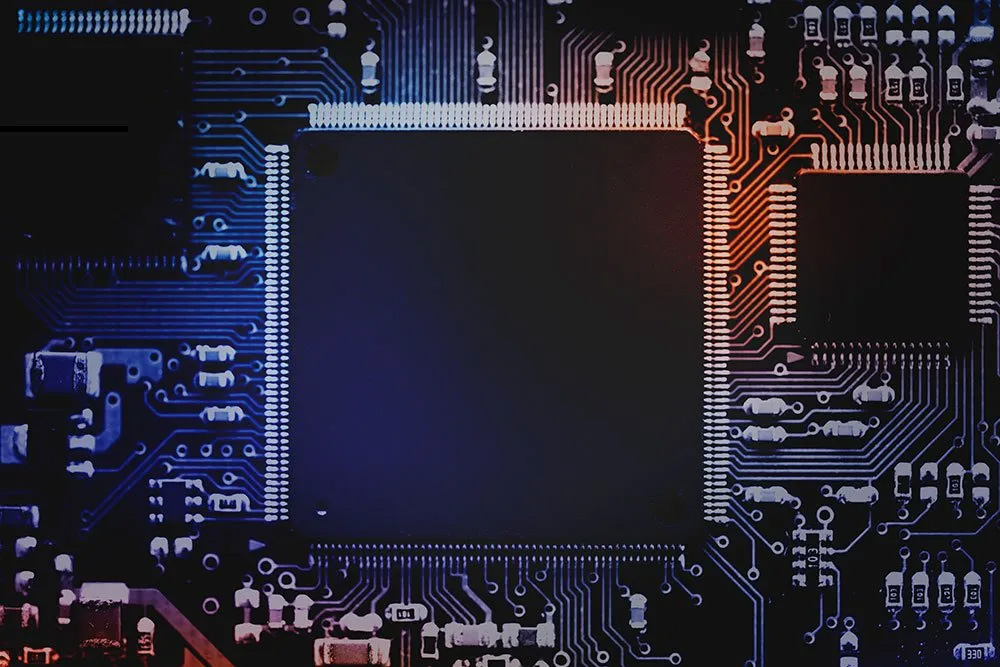
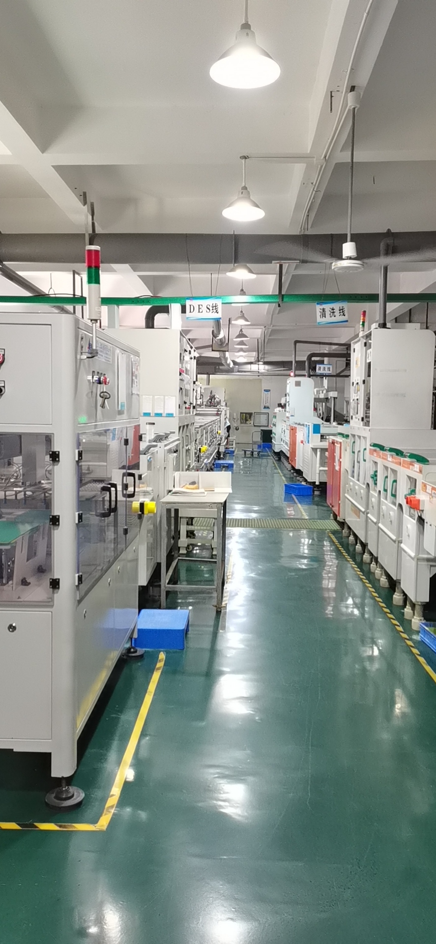
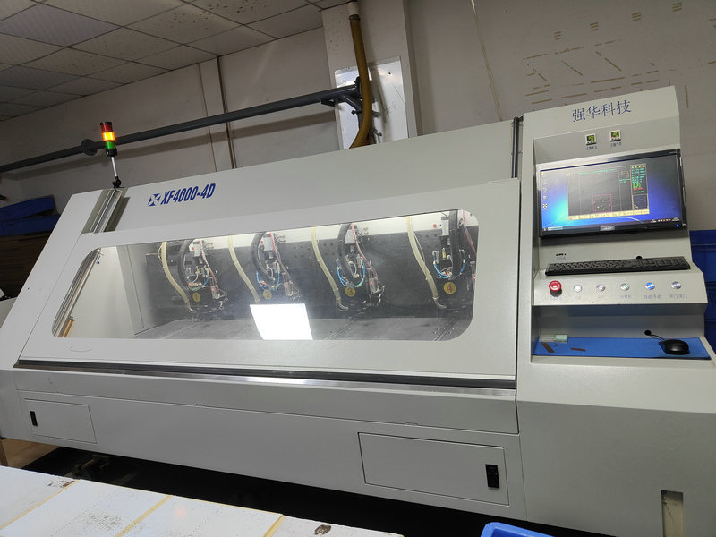
Through hole technology (THT) is a pioneering and mature method that involves inserting pins or leads into printed circuit board holes to connect components. The types of THT devices are grouped according to the configuration of the packaging leads. Radial elements are device types where the leads are perpendicular to the package's long axis, while axial elements are device types where the leads are parallel to the long axis. In THT, wave soldering is a method of soldering lead components into a PCB. Wave soldering is a traditional soldering technique in which the PCB is connected to the component leads and PCB substrate through a molten solder wave.
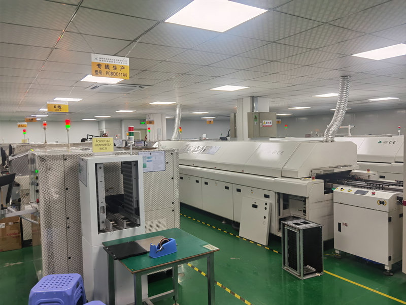
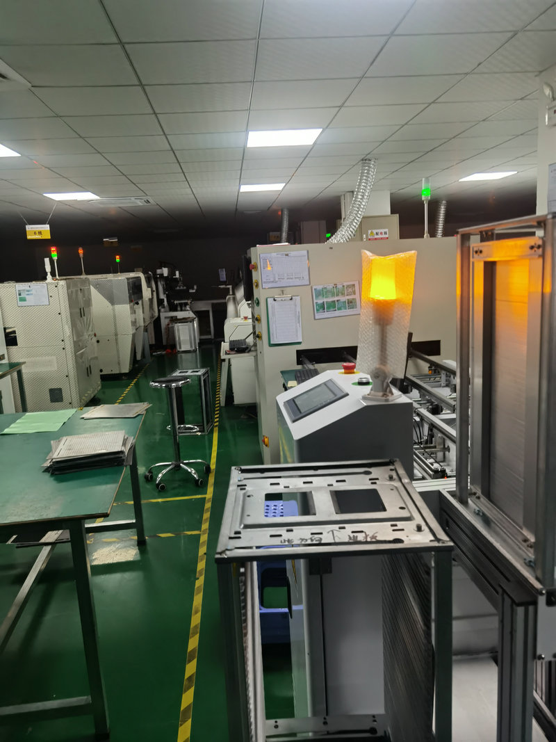
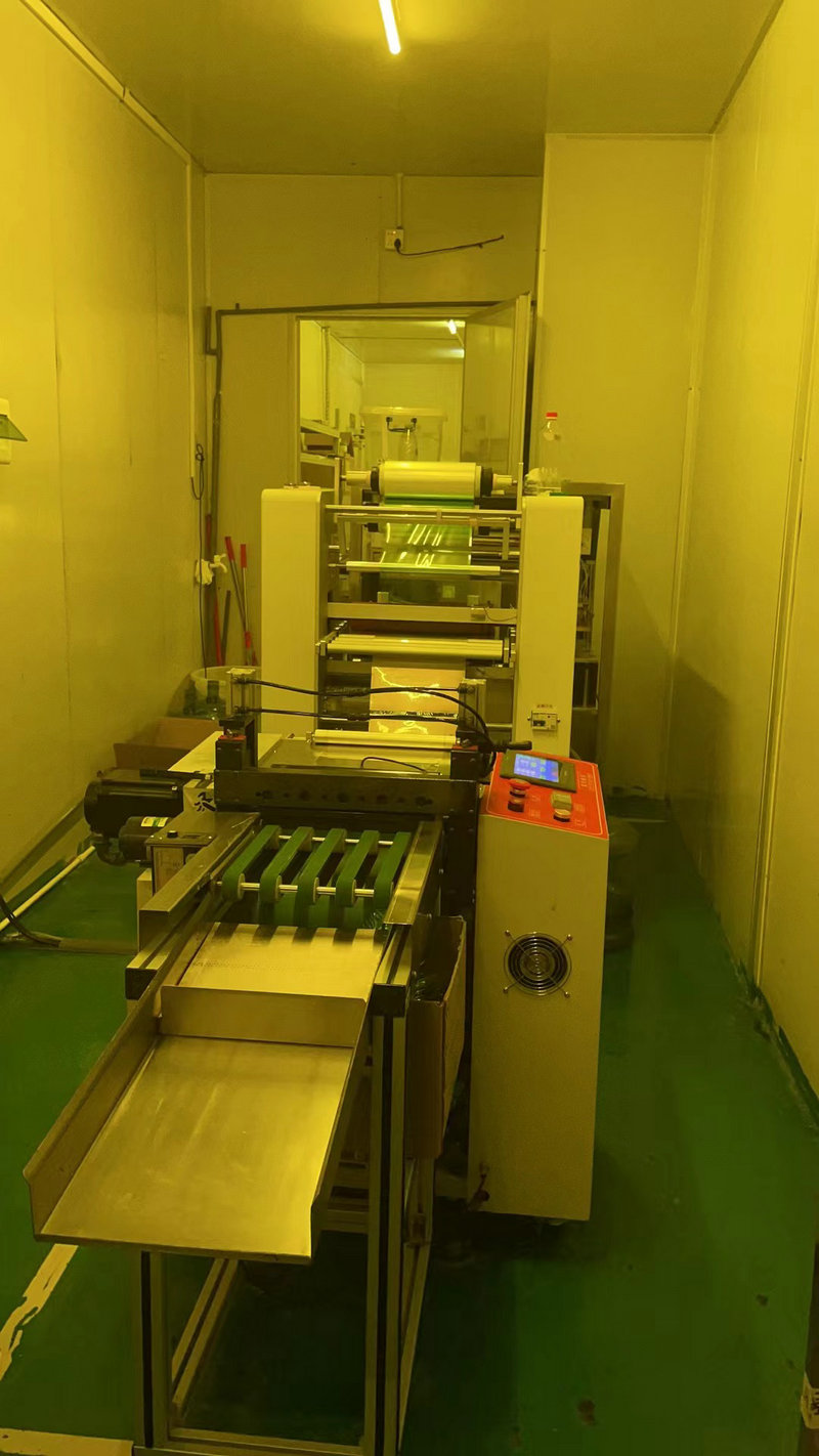
Surface mount technology is a relatively new technology in electronic manufacturing, which refers to the installation of active and passive components on PCBs. SMT utilizes automated machines to achieve efficient production. SMT has the following main processes:
Template printing: Firstly, on the conveyor belt SMT production line, the solder pattern is printed onto the PCB through the template printing process. During the template printing process, the scraper passes through the template opening and evenly deposits solder paste. Templates are usually made of stainless steel material, and their aperture size depends on the amount of solder required. The consistency of solder quantity is the key to achieving a robust template printing process.
Solder Paste Inspection (SPI): Visually inspect the quality of the allocated solder paste using a solder paste testing machine. SPI measures the mounting accuracy and dispensing amount of solder paste. Resolution and threshold settings are parameters that can affect the accuracy of solder paste inspection machines.
Component placement: Electronic components are picked up from the feeder and placed on the PCB at extremely high speeds. SMT machine is a software programmable machine used to control the X, Y, and Z axis movements of the arm for efficient positioning of components. The throughput of a surface mount machine is measured by the number of components per hour, which is usually influenced by factors such as component type and size changes. The main challenges during the component placement process include component missing, misalignment, and bridging. The mounting accuracy is greatly affected by the solder pad pattern, component size, and machine tolerance.
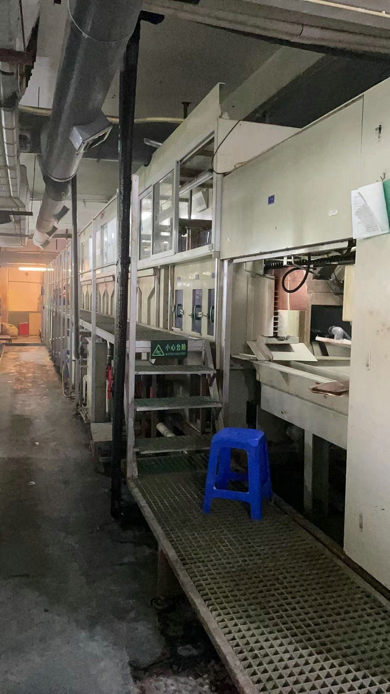
Solder reflow: In order to melt and solidify solder paste, the circuit board needs to pass through a reflow oven composed of heating zones. These heating and cooling steps help achieve connections between PCBs and components. Solder paste material is a filler suspension based on resin, which melts and aggregates during the reflow process.
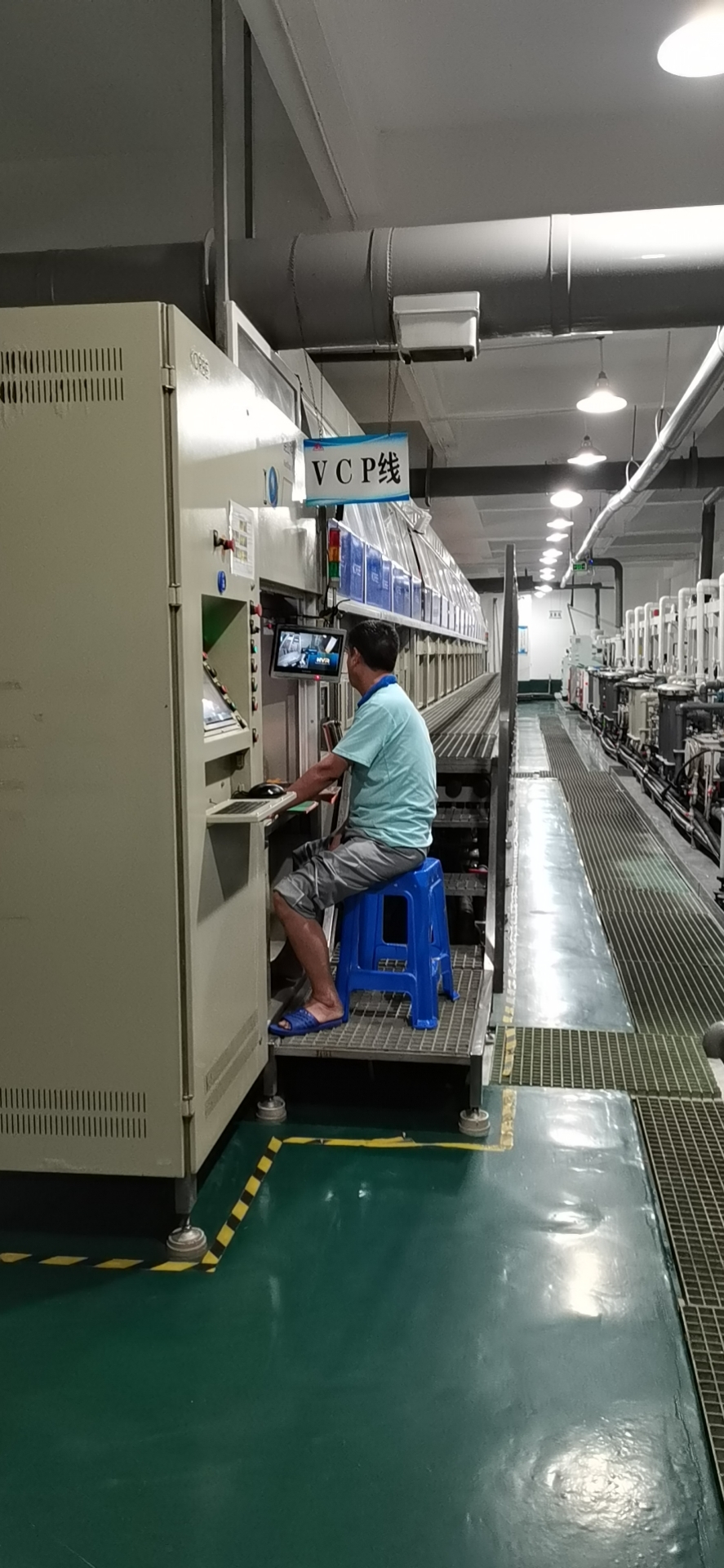
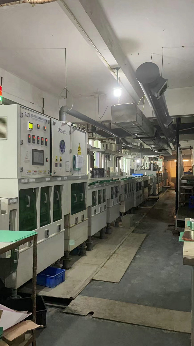
Some PCB designs require the simultaneous use of SMT and THT assembly techniques. Hybrid assembly requires a combination of sequential SMT and THT processes, as well as reflow soldering and wave soldering techniques. This assembly type is typically applied to double-sided panels, where one side has through-hole components and the other side has SMD components.
In mechatronics assembly, the assembled PCB and other mechanical components (such as wires, connectors, power supplies, and sensors) are integrated into a system. The final casing can be customized or ready-made, and should be able to protect the internal electronic components. Advanced robotic machines can be used to precisely assemble the sub components inside the casing.
Some companies also use manual assembly, so strict training and certification of workers are required to meet assembly requirements. The assembly of electromechanical components includes the welding and installation of electrical components, as well as the tightening, insertion, and fastening of mechanical components.
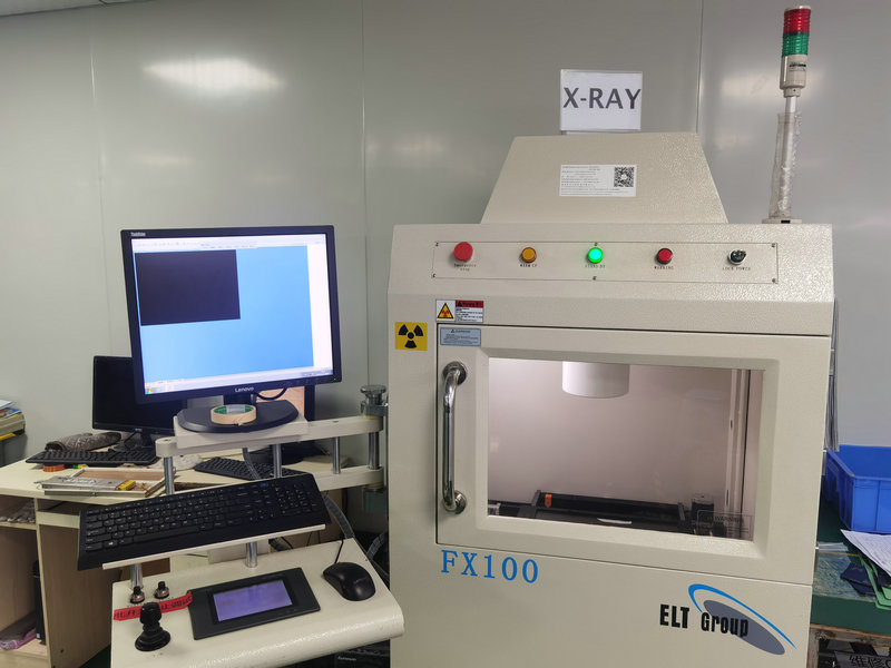
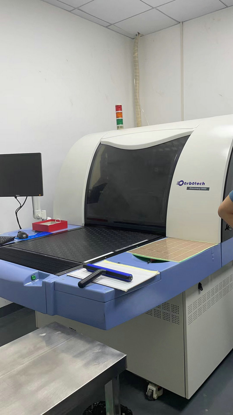
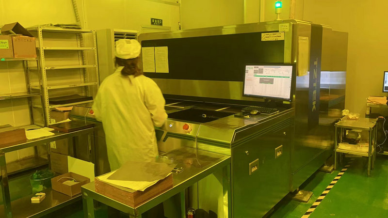
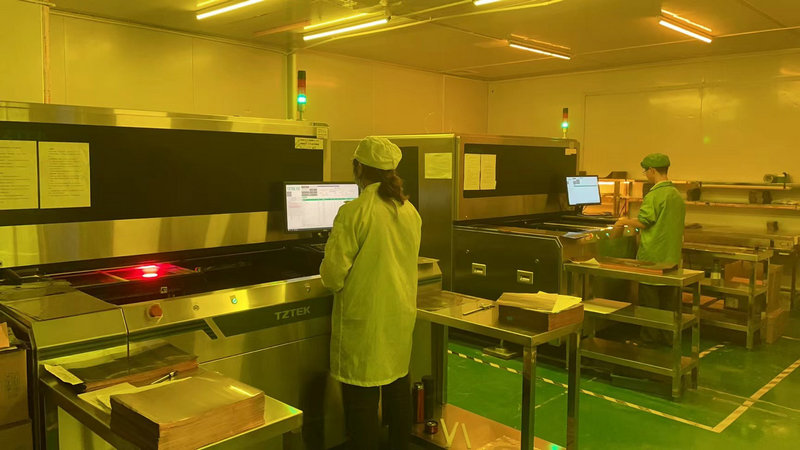
Electronic manufacturing does not end after the manufacturing and assembly process. PCBs and electronic devices must undergo electrical inspection and testing before shipment, as defective products may leak from the production workshop and be transferred to the next process before being delivered to customers. The following are the main inspection and testing processes in electronic manufacturing.
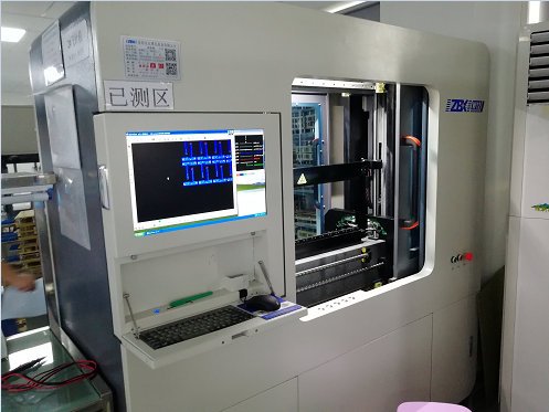
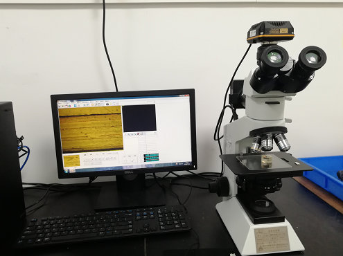
Automatic optical inspection is the process of using visual systems and image processing software to inspect circuit boards and compare them with reference good PCBs. AOI is a reliable technology that has replaced manual inspection, especially for complex components, due to its accuracy and consistency.
Functional testing consists of testing fixtures, connection interfaces, hardware, and software. The testing method is performed by stimulating the product based on its operating environment and checking its response.
Aging testing is also conducted in electronic manufacturing to test finished products. According to the design and application of the product, set the aging furnace with plate slots to a specific temperature. Apply voltage or bias to test the response of components. The duration or hours of aging testing may vary depending on the product. As the distance between devices becomes smaller, establishing an effective interface between the socket and the tested device has become a technical challenge. Aging sockets must adapt to higher currents, frequencies, and pin counts while maintaining low costs and short delivery times. An effective aging testing method should be able to detect potential defects and edge defects, and minimize excessive rejection.
Many OEM brand owners outsource their products to electronic manufacturing service providers mainly because they can quickly manufacture high-quality, competitively priced electronic products without investing in equipment or personnel to establish electronic manufacturing facilities. Then they can focus on design and sales to achieve great success for the brand. Here, we will discuss in detail the benefits of outsourcing electronic manufacturing services.
If you outsource your products, electronic manufacturers will provide you with one-stop service. Including PCB manufacturing, PCB assembly, electromechanical assembly, testing and inspection, and even electronic design, packaging, and distribution. They will handle all the steps for you, especially some difficulties during the process. You don't need to worry about any issues related to the product. Outsourcing electronic manufacturing services to professional large companies with qualified production standards can reduce risks in the production process.
For small and medium-sized companies, the cost of purchasing electronic devices and technology is high, which can be avoided. In addition, if you need to hire personnel to work, it will also cost a lot of money. You still need space to place the equipment. However, if you outsource electronic manufacturing services, you can solve the above problems. Therefore, outsourcing services can help you with cost control and management.
Outsourcing does not mean that you cannot control the quality. On the contrary, outstanding electronic manufacturing service providers typically have strict and rigorous quality control processes. When customers are confident that every finished product has undergone multiple layers of quality inspection, electronic manufacturing services will also be strengthened.
If you encounter difficulties in electronic manufacturing, why not outsource to seek professional engineering support? Engineering support covers many aspects such as original design, prototype design, testing, manufacturing, quality control, maintenance, personnel training, and after-sales service.
Electronic manufacturers are committed to providing customers with first-class and high-quality products and services, achieving a win-win development for both parties.
Quickly bringing products to market is often the key to ensuring competitive success. If your internal production facilities are insufficient, lacking the space, personnel, or equipment needed to shorten the time from initial design to final product, you are at risk of failure.
A partner who can provide flexible facilities and professional personnel, and is qualified to quickly meet your needs, will definitely provide assistance when your product is launched.
Generally speaking, EMS suppliers have very advanced technology, efficient production lines, systematic supply chains, and highly professional personnel settings, and are capable of providing products that meet industry standards.
Choosing the most suitable partner for your electronic manufacturing needs is crucial to achieving your business goals. Trustworthy partners will be the cornerstone of your success. Here are the reasons why our vision can become your best electronic manufacturing service provider.
We, As a Chinese electronic product manufacturer, we have an online quality control and disposal system to respond to major malfunctions and abnormal events. With excellent performance and production technology efficiency, the products and services we provide must be of high quality to meet the requirements of our customers. In addition, we have ISO9001 and UL certifications to ensure that we can provide first-class products.
As is well known, Chinese electronic manufacturing companies are able to provide the best products at the most favorable prices. Compared to short-term benefits, Haibo values long-term mutually beneficial partnerships and does not have a minimum order quantity requirement. You can come to us to request a quote and let us know your preferences so that we can provide the most suitable and budget saving solution on negotiable terms to meet your needs.
Haibo has over 16 years of experience in the field of electronic manufacturing, with skilled engineers and employees who possess the knowledge and ability to produce reliable and high-quality products. The production line has multiple sets of machines that can meet the quality level and requirements of product design. Our electronic manufacturing capabilities include PCB production, PCB assembly, commissioned printed circuit board assembly, turnkey PCB assembly, PCB parts procurement, boxed assembly, integrated circuit programming, functional testing, and more.
Our responsive expert support team is always ready to answer all your questions and keep you informed of order details, ensuring an efficient and effective problem feedback system. We are committed to providing excellent Chinese electronic manufacturing services.
Our products are manufactured using high-speed equipment in an efficient manner
production line. We have a systematic supply chain and logistics system, and with our strong supply chain, experienced employees, and efficient production lines, we can quickly deliver customer orders.
If pursuing cost-effective FPC manufacturing services, choosing a Chinese manufacturer is the best choice. As a manufacturing powerhouse, China has abundant resources, cheap labor, and a large number of technical personnel. We recommend Haibo, a Chinese FPC assembly service provider with over 10 years of experience, who has performed outstandingly in various aspects
Efficient and reasonable quotation:There is an efficient quotation process to assist you in making decisions, providing reasonable prices and highly competitive quotes in China.
High quality and reliable products:Produce high standard printed circuit boards, manufacture and test according to specifications, international standards, and internal controls, and conduct pre production inspections to ensure robust processes.
Quick and on-time delivery:The assembly equipment is in good condition, with high productivity, minimal downtime, short delivery time, and also provides urgent services.
Timely and effective response:Always respond to customer needs, provide accurate information, answer questions through multiple channels, and offer one-stop services.
Strong technical strength:China's FPC manufacturing technology is leading, and Haibo has a complete SMT solution that covers assembly, inspection, and other capabilities. It also provides prototype production and customization services.
mobile phone: 86-15113315665
Contact: Chen Changhai
mobile phone: 86-18676922028
E-mall: haibo_fpcba1668@163.com
Address: 3rd Floor, Building 2, Fuxing Industrial Park, Building B, Chuangye 1st Road, Jiangbian Community, Songgang Street, Bao'an District, Shenzhen