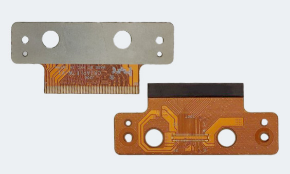
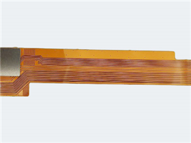
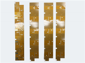
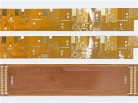
The manufacturing process of multi-layer impedance FPC is relatively complex, requiring high-precision process control and advanced production equipment. It mainly includes the following steps:
Inner layer circuit fabrication: Inner layer circuits are fabricated on the substrate, and predetermined circuit patterns are formed through processes such as photolithography and etching.
Layering and Drilling: The produced single-layer circuit board is laminated according to design requirements to form a multi-layer structure. Then, precision drilling equipment is used to drill holes at the required locations in preparation for subsequent electrical connections.
Electroplating and impedance control: Electroplating treatment is performed after drilling to form a conductive layer. At the same time, precise control of circuit characteristic impedance can be achieved by adjusting electroplating parameters and selecting insulation layer materials.
Surface treatment and cover film bonding: Apply anti-oxidation treatment to the surface of the multi-layer board and bond the cover film at designated locations to protect the circuit from short circuits and external environmental influences.
Forming and inspection: After cutting, bending and other steps, the FPC circuit board is finally formed according to the product form requirements, and undergoes strict quality inspection to ensure compliance with design and usage standards.
mobile phone: 86-15113315665
Contact: Chen Changhai
mobile phone: 86-18676922028
E-mall: haibo_fpcba1668@163.com
Address: 3rd Floor, Building 2, Fuxing Industrial Park, Building B, Chuangye 1st Road, Jiangbian Community, Songgang Street, Bao'an District, Shenzhen