Design and Manufacturing Process of Capacitive PCB
Design Considerations
Key factors affecting design:
Sensitivity: The sensitivity of the capacitive sensor PCB depends on the intended use, including sensitivity and resolution, as well as other functional requirements.
Device size and shape: Due to its compact size and shape, the integration of capacitive characteristics poses a challenge.
Power consumption: Considering that most products are battery powered devices, these designs must achieve an ideal balance between optimal response capability and power efficiency.
The importance of layout and spacing
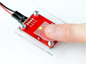
Electrode configuration: The electrode arrangement must be correct in order to detect touch correctly. Overlapping or approaching electrodes can cause signal interference.
Line width and spacing: Reduce the line width and increase the line spacing to minimize capacitive coupling and improve performance.
Overview of Manufacturing Process
Material selection: Firstly, select substrates and conductive materials that meet the specifications for capacitance and durability design.
Layer stacking: When stacking layers, care must be taken, and the order of conductive and dielectric layers must be precise. This process is very precise and crucial for the normal operation of the PCB.
Etching: The pattern of traces and electrodes is achieved by eliminating conductive materials. This operation must be completed very accurately to preserve the design.
Testing: All circuit boards have undergone functional performance testing; Some circuit boards have also undergone capacitance characteristic and response accuracy testing.
Specific challenges in production
Etching accuracy: The required accuracy for capacitance characteristics is very high, so it is very difficult to achieve such a level of accuracy. Ultimately, it is likely to incur significant production costs.
Material consistency: The difference between dielectric materials and conductive materials can affect the capacitance level, therefore strict quality control measures are required.
Component integration: The assembly of capacitive PCB and other electronic components should be carried out in such a way that its assembly does not have any impact on the capacitance characteristics of the PCB.
The design and manufacturing of capacitive PCBs combine technical knowledge, precise engineering, and strict quality control to ensure that the final product meets the specific needs of touch devices.
Your trusted partner and one-stop supplier for FPC/PCB manufacturing, component procurement, FPC/PCB assembly, and electronic manufacturing. With over 16 years of experience, we have been providing high-quality FPC/PCB at competitive prices to over 1000 customers worldwide. Our company has passed ISO9001:2015 certification and UL certification, and all of our products have undergone 100% electronic testing and passed AOI and X-RAY inspections to meet the highest industry standards. Therefore, please obtain an immediate quote from our sales team as we will handle the remaining matters.
Haibo is an expert in the field of FPC/PCB manufacturing and surface mount assembly in China. Since our establishment in 2017, we have been providing high-quality PCBs to over 1000 customers worldwide. Our factory has passed ISO14001, ISO9001:2015, TS16949, and ISO13485:2016 certifications. We are one of the most trusted small and medium-sized FPC/PCB manufacturers in China.